2. Basic Development Courses
2.1 Controller Hardware Course
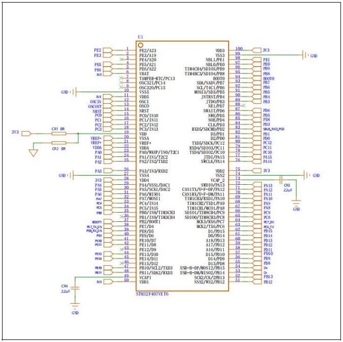
2.1.1 ROS Robot Controller Hardware Introduction
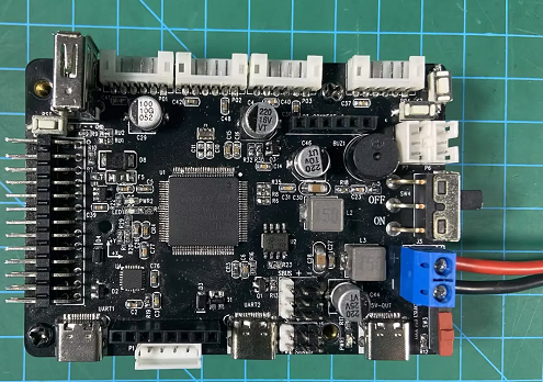
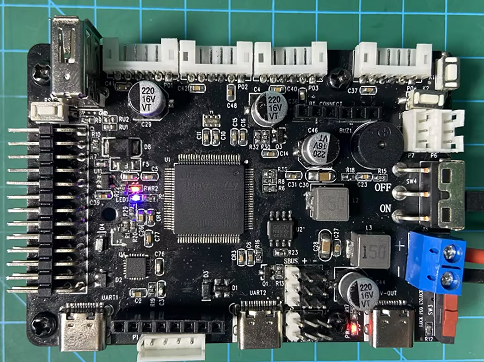
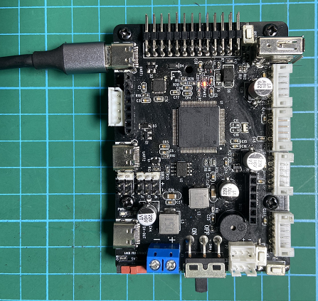
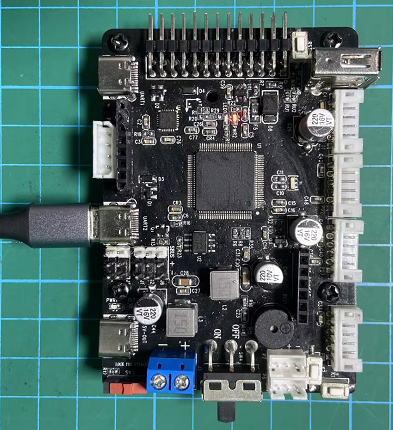
Development Board Diagram
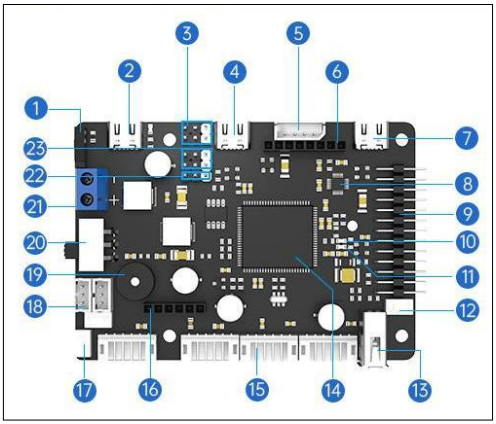
| NO. | Function Description |
|---|---|
| 1 | Motor control switch: When turned on, the motor can move; when turned off, the motor is not controlled |
| 2 | 5V 5A external power supply: Specially designed to power Raspberry Pi, Jetson Nano development boards, etc. |
| 3 | Battery voltage powered PWM servo interface x2: For high current and high torque servo control |
| 4 | USB serial port 2: Designed for serial communication interface to communicate with Raspberry Pi and Jetson Nano. |
| 5 | I2C expansion interface: Can be used for module communication of the I2C interface. |
| 6 | 0.96-inch LCD display interface: For LCD display module. |
| 7 | USB serial port 1/burning download: Can be used for program serial port burning and serial port communication. |
| 8 | MPU6050 IMU attitude sensor: Provides the current attitude of the development board. |
| 9 | GPIO expansion and SWD debugging: Used for other expansion external modules and debugging. |
| 10 | User indicator light: Allows users to customize LED light functions. |
| 11 | Power indicator light on the board: Indicates whether the voltage of each part is normal. |
| 12 | Reset button: Main control chip reset button. |
| 13 | USB HOST interface: Can connect USB slave devices such as USB handle receivers. |
| 14 | STM32F407VET6 main control chip: Main frequency 168MHz, ARM Cortex-M4 core, Flash 512KB, RAM 192KB, 82 general IO ports. |
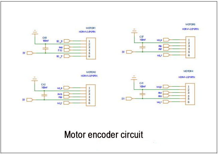
| 15 | Four-lane encoded motor interface x4: Can drive four motors simultaneously. Refer to the corresponding course documents for connection methods based on different models. |
| 16 | Bluetooth module interface: Can receive control instructions from mobile apps, other Bluetooth modules, etc. |
| 17 | User button x2: Allows users to customize key functions and combined key functions. |
| 18 | Bus servo interface x2: Can control the movement of the bus servo mechanical arm. |
| 19 | Buzzer: Used for user prompts and alarm functions. |
| 20 | Power switch: Main power switch of the development board. |
| 21 | Power interface: DC 5V ~ 12.6V power input, can be powered by a power supply or battery. |
| 22 | SBUS remote control receiver interface: Used to connect model aircraft remote control receiver. |
| 23 | 5V power supply PWM servo interface x2: Can be used for 5V servo control. |
FAQ for Controller
How to control the control board with Raspberry Pi and Jetson Nano? How to communicate with the control board?
Answer: Raspberry Pi, Jetson Nano, and similar devices can communicate with the control board via the serial port. It is recommended to use serial port 2 for communication to keep serial port 1 available for downloading programs. This reduces the need for frequent plugging and unplugging, speeding up the debugging process.
Which functions on the development board are managed by the microcontroller?
Answer: The microcontroller on the development board manages several components, including the buzzer, robotic arm, servo gimbal, button, Bluetooth module interface, encoder motor interface, USB HOST interface, LED, MPU6050 attitude sensor, USB serial port, display interface, I2C interface, SBUS interface, GPIO expansion port, and more.
How to learn to use the development board? How to update the development board firmware?
Answer: The development board comes with comprehensive tutorials, such as the FREERTOS system LED control tutorial, encoder motor control tutorial, and motor PID control tutorial. Interfaces are pre-implemented to facilitate rapid development. To update the firmware, you can use the USB serial port for downloads and JLink for debug updates. All interfaces are externally connected to make learning and debugging easier.
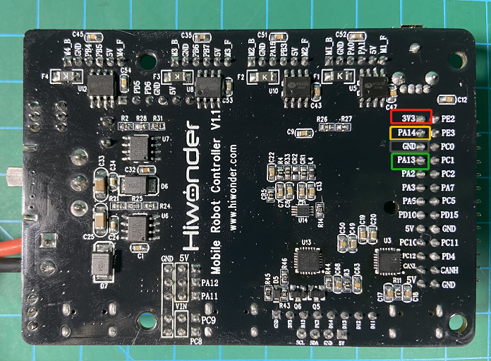
Why are two pins of the main control chip STM32F407VET6 on the development board connected?
Answer: First, check if the version silk screen on the back of the board is V1.0. If it is version V1.0, it is normal for the two pins to be connected as shown in the figure below. In the V1.0 version, one pin is VDD and the other is related to the chip’s built-in voltage measurement standard. These pins need to be connected to correctly read the battery voltage value. In version 1.1, this chip does not require pin soldering.
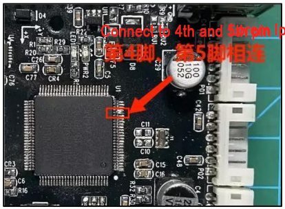
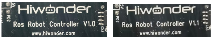
(Left: V1.0; Right: V1.1)
2.1.2 ROS Robot Controller Schematic Explanation
Main Chip Description
Main chip: STM32F407VET6
This STM32F407VET6 has 100 pins. As you can see, many of these pins are already in use, while others are left available for customers to use in their own development. Below, we will detail which pins are in use, their functions, and which pins are available.
Shut Capacity
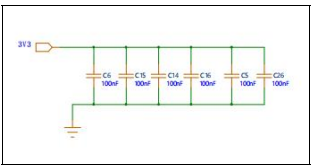
These 100nf capacitors are connected to the 3.3V supply on the STM32F407VET6. The functions of these bypass capacitors are voltage stabilization and filtering.
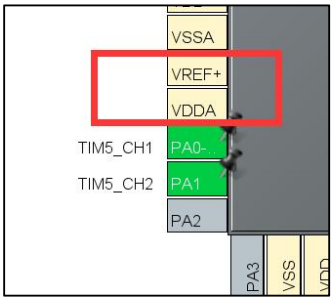
Peripheral Circuitry of the VET6
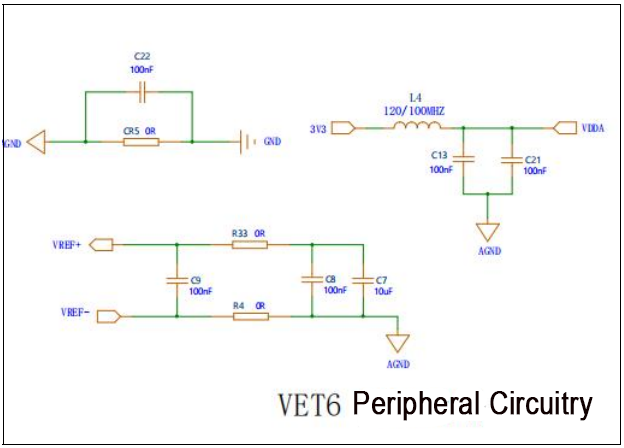
In the peripheral circuit of the device, the connections between AGND (analog ground) and GND (digital ground) and between 3V3 and VDDA play important roles. Analog and digital signals often need to coexist on the same circuit board, and the switching processes of digital circuits can introduce noise. Typically, two separate systems are used: one for the analog circuit (AGND) and one for the digital circuit (GND), to minimize interference between the ground currents of the analog and digital parts while ensuring consistent potential throughout the system to minimize noise impact.
3V3 is the supply voltage, and VDDA is the analog supply voltage. The circuit design may include power supply decoupling devices. An LC filter is formed by connecting an inductor (L) and two 100nF capacitors (C) in parallel. This filter reduces high-frequency noise in the supply voltage, thereby providing a more stable analog supply voltage (VDDA). This is crucial for power supply decoupling of peripheral circuits.
VREF+ and VREF- are connected in parallel with two 100nF capacitors, known as decoupling capacitors. These capacitors reduce high-frequency noise on power lines, smooth the power supply voltage, and provide a more stable voltage.
Additionally, a 10uF capacitor is connected to AGND through two 0-ohm resistors. This method of power supply filtering allows the 10uF capacitor to provide low-frequency decoupling. The 0-ohm resistors offer a low-impedance path between the power line and the ground line, helping to reduce the impact of power supply noise on the voltage. This improves the accuracy and performance of ADC and DAC circuits.
Power Indicator
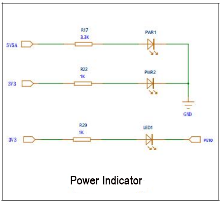
The three circuits of the power indicator light utilize resistors to regulate the current flowing through the LED, thus preventing overheating and damage to the LED.
In the first circuit, powered by a 5V supply, a 3.3k resistor is connected in series with the LED to ground. By applying Ohm’s law (I = V/R), the current (I) flowing through the circuit can be calculated as I = 5V / 3.3kΩ = 1.52mA. This current value falls within the safe operating range, as the maximum continuous operating current for most LEDs is approximately 20mA.
In the second circuit, powered by a 3.3V supply, a 1k resistor is used in series with the LED to ground. Similarly, the current can be calculated as I = 3.3V / 1kΩ = 3.3mA, which is also within the safe range.
In the third circuit, this connection method is typically employed to indicate a specific status of the main chip. When the PE10 pin is configured as a low output, current flows through the LED and resistor to ground (GND), illuminating the LED. Conversely, when the PE10 pin is configured as a high-level (3.3V) output, the voltage difference across the LED is 0, causing the current to cease flowing and the LED to turn off.
Crystal Oscillator Circuit
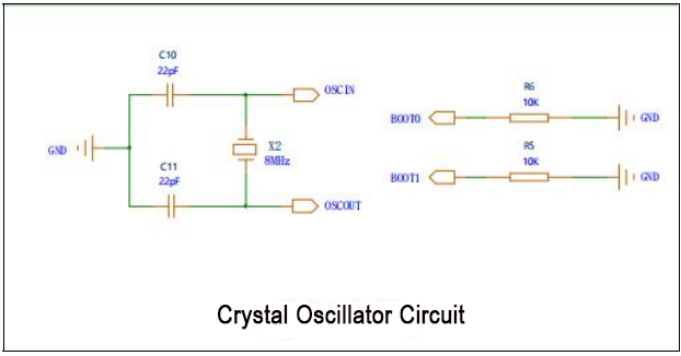
An 8MHz crystal is paralleled with the OSCIN and OSCOUT pins on the STM32F407VET6 chip. Each crystal oscillator pin is accompanied by a 22pF capacitor, connected to the ground wire, forming a loop crucial for initiating crystal oscillation, ensuring a stable clock signal.
Regarding BOOT and BOOT1, they serve as digital input pins to determine startup configurations upon power-on or reset. By reading the levels (high or low) at these pins, different boot sources are selected accordingly. Options include booting from built-in Flash memory, system memory, or an external memory device. Both BOOT0 and BOOT1 pins are linked to ground via 10KΩ resistors, ensuring they default to a low level during power-up or reset, typically establishing the default startup mode.
For example, the system can boot from built-in Flash memory, system memory, or an external memory device. The BOOT0 and BOOT1 pins are grounded through a 10KΩ resistor each. This means that upon power-up or reset, these pins will be pulled low (set to a low level). The purpose of this configuration is typically to set the default boot mode.
Button Circuit
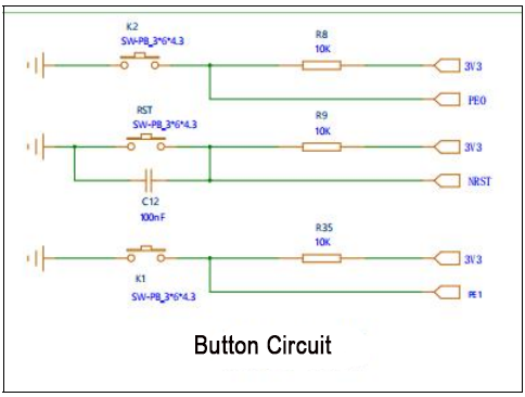
These three circuits are pull-down resistor button circuits. When the button is not pressed, the PE0 pin is connected to the 3.3V power supply through a 10kΩ resistor, so the PE0 pin reads a high level. When the button is pressed, the PE0 pin is directly grounded, so the PE0 pin reads a low level.
The NRST reset button and the PE1 circuit work the same way.
OLED Display
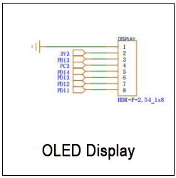
This socket connects to the OLED display, interfacing with the PB13, PC3, PD14, PD13, PD12, and PD11 pins of the STM32F407VET6. You can view its configuration through the program and refer to the STM32F407VET6 specification sheet in the folder to see the functions shared by these pins.
Bluetooth Module Port
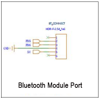
This is a screen holder connected to the Bluetooth module interface. It connects to the PD5 and PD6 pins of the STM32F407VET6. You can view the configuration through the program and refer to the STM32F407VET6 specification folder to see the functions these pins perform.
IIC Reserved Port
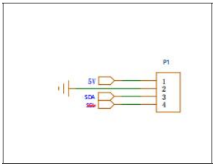
This is an IIC reserved interface that can be connected to external IIC devices, such as language modules and OLED screens. The IIC pins of the STM32 are connected here, and the IIC bus is pulled up on the MPU6050.
SWD Download
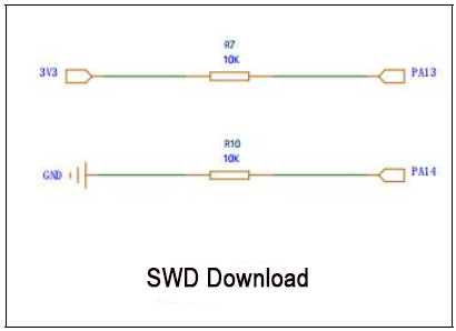
In the STM32F407VET6 chip, the two pins are typically used as a debug port (SWD interface), with PA13 serving as SWDIO (data line) and PA14 as SWCLK (clock line).
Reserved Port
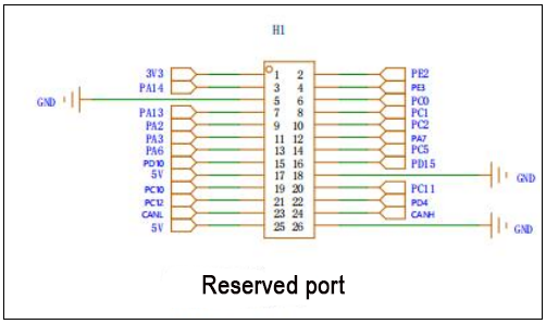
The reserved interface consists of GPIO ports on the STM32F407VET6 main chip that have not yet been used.
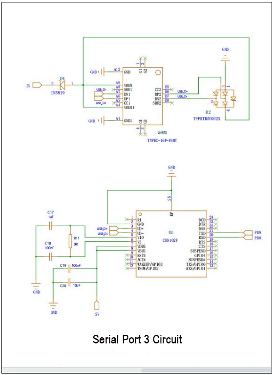
TYPEC Port
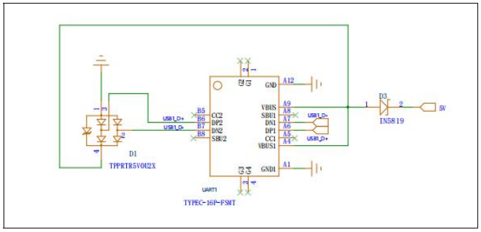
Connect a diode to VBUS to prevent reverse current on the VBUS line.
The cathode of the diode is connected to the VBUS pin, and the anode is connected to the power circuit.
This way, the power circuit can draw power from the VBUS pin but cannot supply power back to the VBUS line.
DP2 and DN2 are the differential data lines of the USB Type-C connector used for transmitting USB data. Connecting an ESD protection device can prevent these lines from being damaged by electrostatic discharge (ESD) or other overvoltage events.
MPU-6050
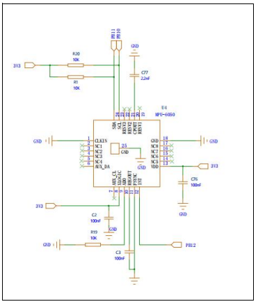
Here, both the SCL and SDA pins of the MPU-6050 are connected to 10k pull-up resistors, facilitating their functionality as pull-up resistors. Consequently, the device can pull the line low but cannot actively pull it high.
Power connection: The VCC pin of the MPU-6050 requires connection to a 3.3V power supply, while the GND pin should be linked to ground.
I2C signal line connection: SDA and SCL represent crucial lines for I2C communication, serving as data and clock lines respectively. Correspondingly, the pins associated with I2C functionality are connected to SDA and SCL on the MPU-6050. For instance, on the STM32F407VET6, PB11 can serve as SDA, and PB10 can function as SCL.
Interrupt pin: The INT pin acts as an interrupt output. It facilitates communication between the MPU-6050 and the STM32F407VET6 chip by signaling new data availability or other relevant events.
Capacitor integration: When the MPU-6050 initiates operation and draws current from the power line, the integrated capacitor swiftly furnishes the necessary current, mitigating momentary drops in the supply voltage. Simultaneously, the capacitor serves to attenuate high-frequency noise on the power line, safeguarding the MPU-6050 against noise-induced performance disruptions.
CH9102F Serial Port 3 Circuit
Here, both the SCL and SDA pins of the MPU-6050 are connected to 10k pull-up resistors, facilitating their functionality as pull-up resistors. Consequently, the device can pull the line low but cannot actively pull it high.
Power connection: The VCC pin of the MPU-6050 requires connection to a 3.3V power supply, while the GND pin should be linked to ground.
I2C signal line connection: SDA and SCL represent crucial lines for I2C communication, serving as data and clock lines respectively. Correspondingly, the pins associated with I2C functionality are connected to SDA and SCL on the MPU-6050. For instance, on the STM32F407VET6, PB11 can serve as SDA, and PB10 can function as SCL.
Interrupt pin: The INT pin acts as an interrupt output. It facilitates communication between the MPU-6050 and the STM32F407VET6 chip by signaling new data availability or other relevant events.
Capacitor integration: When the MPU-6050 initiates operation and draws current from the power line, the integrated capacitor swiftly furnishes the necessary current, mitigating momentary drops in the supply voltage. Simultaneously, the capacitor serves to attenuate high-frequency noise on the power line, safeguarding the MPU-6050 against noise-induced performance disruptions.
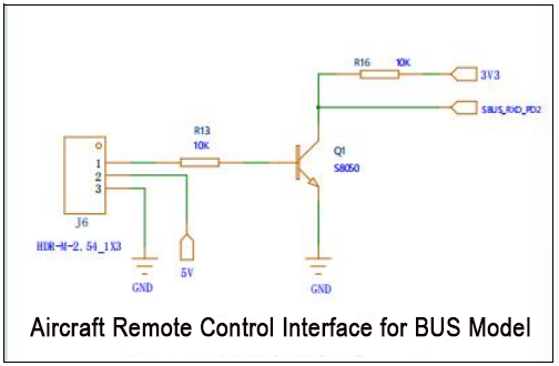
Aircraft Remote Control Interface for BUS Model
This serves as the remote control interface for the BUS model aircraft. An NPN transistor functions as the inverter in this setup. When the SBUS signal is at a high level, the transistor conducts, pulling the output low. Conversely, when the SBUS signal is low, the transistor switches off, and a pull-up resistor raises the output to a high level. This configuration yields the inverted SBUS signal. To receive and transmit this signal to the main chip, connect the PD2 pin of the main chip accordingly.
CAN Port
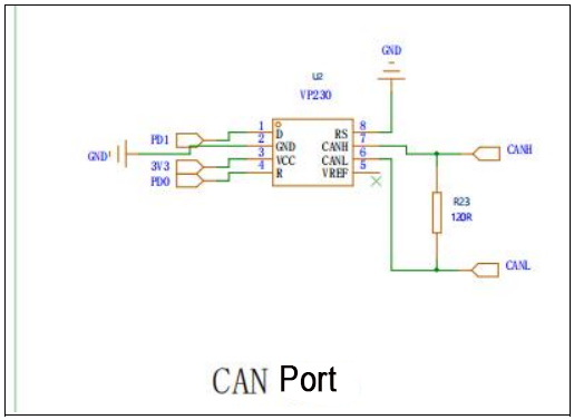
The CAN interface is linked to a 120-ohm resistor. This resistor serves as the terminal resistor for CAN communication, aiding in impedance matching and mitigating echo emissions.
Buzzer
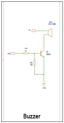
One end of the buzzer is connected to a 5V power source, and the other end is linked to the collector of an S8050 transistor. The collector is grounded through a 10kΩ resistor.
The base of the transistor is connected to the PA4 pin of the microcontroller via a 1kΩ resistor.
When you want the buzzer to sound, you can set the PA4 pin of the main chip to output a high level, which turns on the transistor, allowing current to flow through the buzzer and producing sound. When you want the buzzer to stop sounding, you can set the PA4 pin to output a low level, which turns off the transistor, cutting off the current flow through the buzzer and stopping the sound. This buzzer serves as an external device.
Enable Switch
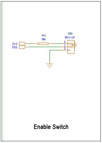
This switch is used to control the car to stop.
4-Lane Servo Port
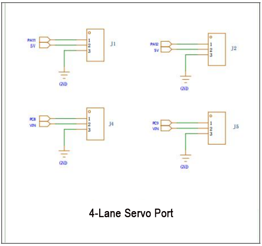
These four interfaces are designated for connecting servos, enabling servo control. There are two servo sockets connected to the 5V power source and two servo sockets connected to VIN. The 5V socket is intended for low-voltage servos, while VIN is designated for high-voltage servos powered by a high-voltage power supply.
5V-TO-3.3V Circuit
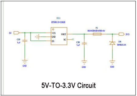
The BSMD0603-050-6V is a fuse connected to the output terminal of the RT9013-33GB. It protects against damage from excessive current. When the current exceeds the rated value of the fuse, it will disconnect, thereby cutting off the current flow.
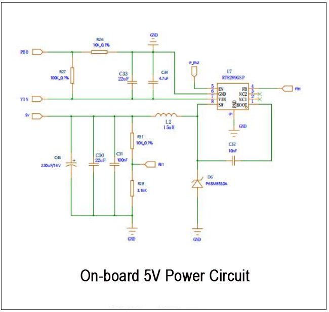
Raspberry Pi 5V Power Supply Circuit and Onboard 5V Power Circuit
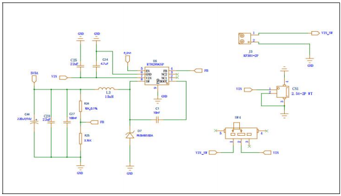
As the name implies, this circuit supplies power to our Raspberry Pi using an RT8389GSP power chip. The output, 5V5A, can be adjusted via R24 and R25 according to the formula: V_OUT = V_FB * (1 + R1/R2). Here, V_OUT represents the regulator’s output voltage, while V_FB denotes the feedback reference voltage, typically a fixed value internally set in the regulator, often around 1.222V. (For further details, consult the RT8289GSP manual if interested.) SW4 serves as the control switch. Simultaneously, this circuit functions as an onboard 5V power supply, adjustable similarly to the aforementioned setup.
On-board 5V Power Circuit
Simultaneously, a TYEC is employed to link 5V5A to the Raspberry Pi power supply circuit. Additionally, a 10k resistor and capacitor are combined to create a low-pass filter, aiding in the elimination of high-frequency noise. Finally, a 0-ohm jumper resistor connects both P_EN and VIN.
Motor Drive Circuit
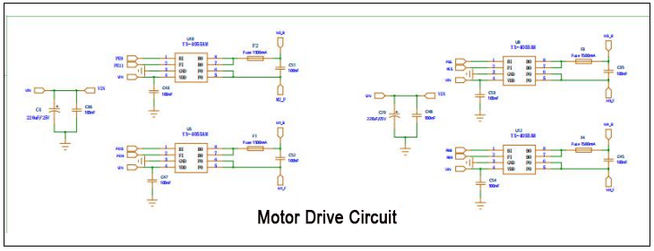
Here, we utilize the YX-4055AM motor driver chip to manage four motors. The chips, namely PE9, PE11, PE5, PE6, PE13, PE14, PB8, and PB9, connected to the main chip, regulate our motor rotation, speed, and other functions. Furthermore, a 1500mA fuse has been added to the BO output of the motor driver chip to prevent potential chip damage due to excessive current and voltage.
Additionally, capacitors C4, C36, C29, and C48 serve the purposes of filtering and denoising. These capacitors act as filters, aiding in noise reduction along the power line. Specifically, a 220uF capacitor effectively mitigates low-frequency noise, while a 100nF capacitor excels at removing high-frequency noise.
Moreover, these capacitors play a crucial role in stabilizing the supply voltage. Fluctuations in load current can cause voltage instability, but the capacitors step in to provide the necessary current, thus stabilizing the power supply voltage and preventing voltage transients. Additionally, they prevent the power supply peak current from reaching excessively high levels. When the circuit experiences sudden demand for a large current, the capacitors supply this additional current, preventing spikes in power supply current that could otherwise impact the system.
Lastly, the following section outlines the interface for our encoded motor, which connects to the output pin of the motor driver chip and undergoes filtering via a 100nF capacitor.
Serial Bus Servo Port
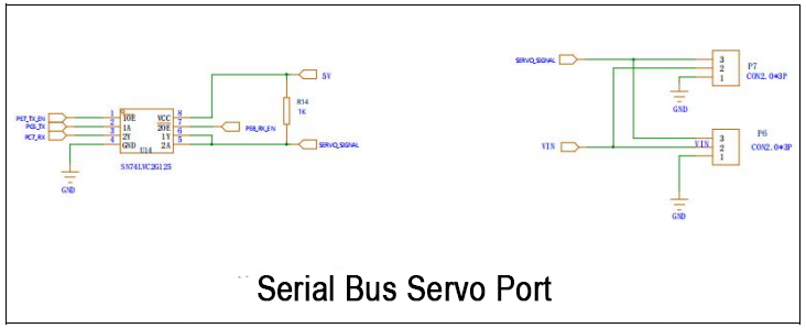
This circuit and interface correspond to our bus servo. PE7, PG6_TX, and PC7_RX are connected in series to the main chip.
USB_HOST Port Circuit
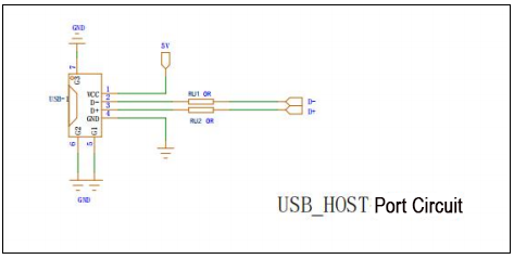
D- and D+ are connected to the main chip via PB15 and PB14, with a jumper resistor in between. These connections receive the signal from the controller and then transmit it to the STM32 chip for decoding and processing.
2.2 STM32 Development Fundamentals
2.2.1 Development Environment Setup
 After installing the Keil software, please activate it. Otherwise, compilation failures may occur, affecting normal usage.
Keil Software Installation
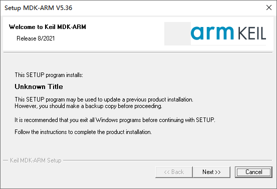
Keil is specialized software designed for microcontrollers, with powerful functionality. Regardless of the version, the installation process is the same. This section uses V5.36 as an example:
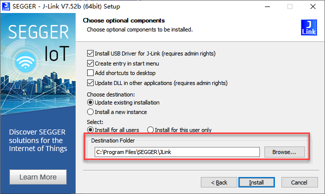
Go to the folder ‘Keil Installation Package and mcuisp Download Tool’, double-click the ‘mdk536.exe’ file.
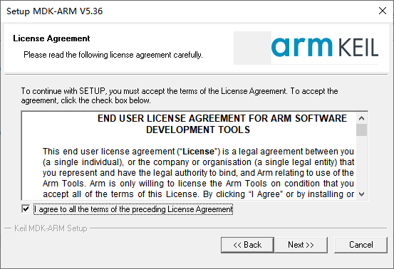
Check the options and agree to the installation agreement.
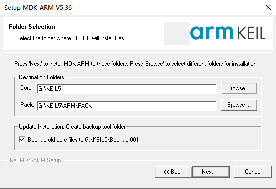
Choose the installation path.
User information needs to be filled in here, you can fill it in randomly.
After filling in, click ‘Next’ to proceed with the installation.
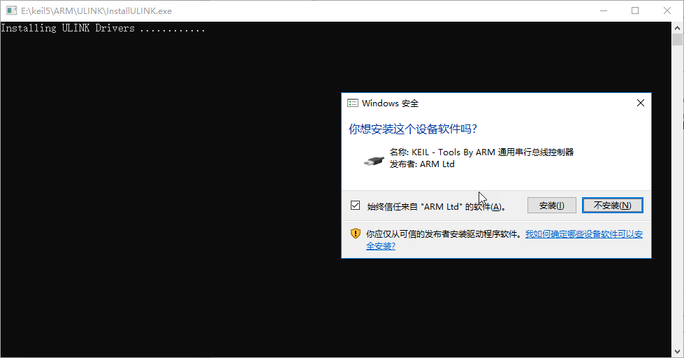
Wait for a moment, a prompt to install the ULink driver will pop up, click ‘Install’ at this time.
After the installation is complete, click ‘Finish’ to exit.
Configuration
1. Add Chip Support Package
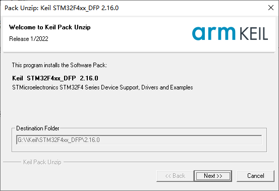
After installing the Keil 5 software as described earlier, we need to manually install the required chip package, which can be found in this section’s directory.
After opening it, click ‘Next’.
Wait for the installation to be completed, then click-on ‘Finish’ button.
Reopen the Keil software, then click-on pack installer icon.
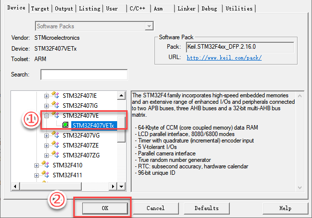
Click-on ‘Device’ button. Then choose the correct device as pictured.
2. Install J-Link Driver
J-Link is a commonly used debugger/emulator, used for microcontroller development and debugging in conjunction with Keil 5. Therefore, when using J-Link for programming and debugging microcontrollers in Keil 5, it is necessary to install the J-Link driver.
You can find the J-Link installation package in this section’s directory, then double-click to open it, and click ‘Next’.
Choose ‘I Agree’.
Select the installation path to be the same directory as Keil 5.
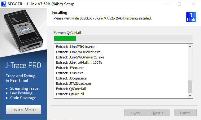
Wait for the installation to be completed.
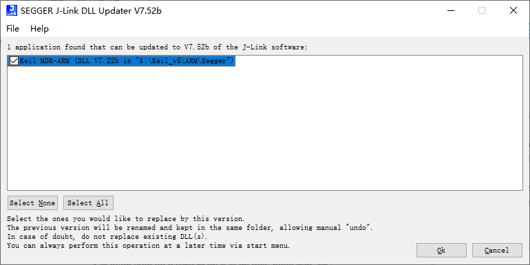
Installation completed. If a prompt for upgrade appears, as shown in the following image, simply close it.
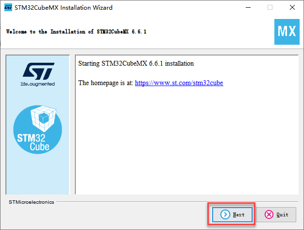
Install STM32CubeMX
STM32CubeMX is a graphical tool for configuring STM32 microcontrollers. It assists developers in quickly configuring peripherals such as clocks, GPIOs, interrupts, DMA, etc., and generates initialization code. It supports various development environments, including Keil, IAR, and GCC.
The installation package can be found in this section’s directory. Double-click to open it, and click ‘Next’.
Tick ‘I accept the terms of this license agreement’, and click-on ‘Next’ button.
You must check the first option above, then click ‘Next’.
Select the installation path, ensuring that the path does not contain any Chinese characters. Then continue by clicking ‘Next’ and wait for the installation progress bar to complete.
After waiting for the installation to complete, continue by clicking ‘Next’, then click ‘Done’ to finish.
2.2.2 Light up LED
Preface
This lesson will use software to write a program for the LED on the STM32 main control board, controlling the onboard LED to blink.
Preparation
1. Software Preparation
Keil5 and related environment configuration (if not installed or configured, installation methods can be found in “2.2.1 Development Environment Setup”).
J-Link firmware installation (if not installed or configured, installation methods can be found in “2.2.1 Development Environment Setup”) for burning.
2. Hardware Preparation
STM32 Main Controller
The Jlink debugger and a Micro-USB data cable (self-provided) are used for code flashing.
Operation Steps
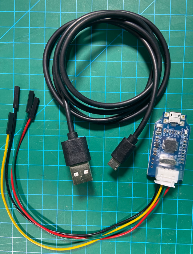
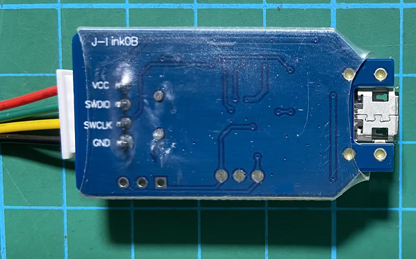
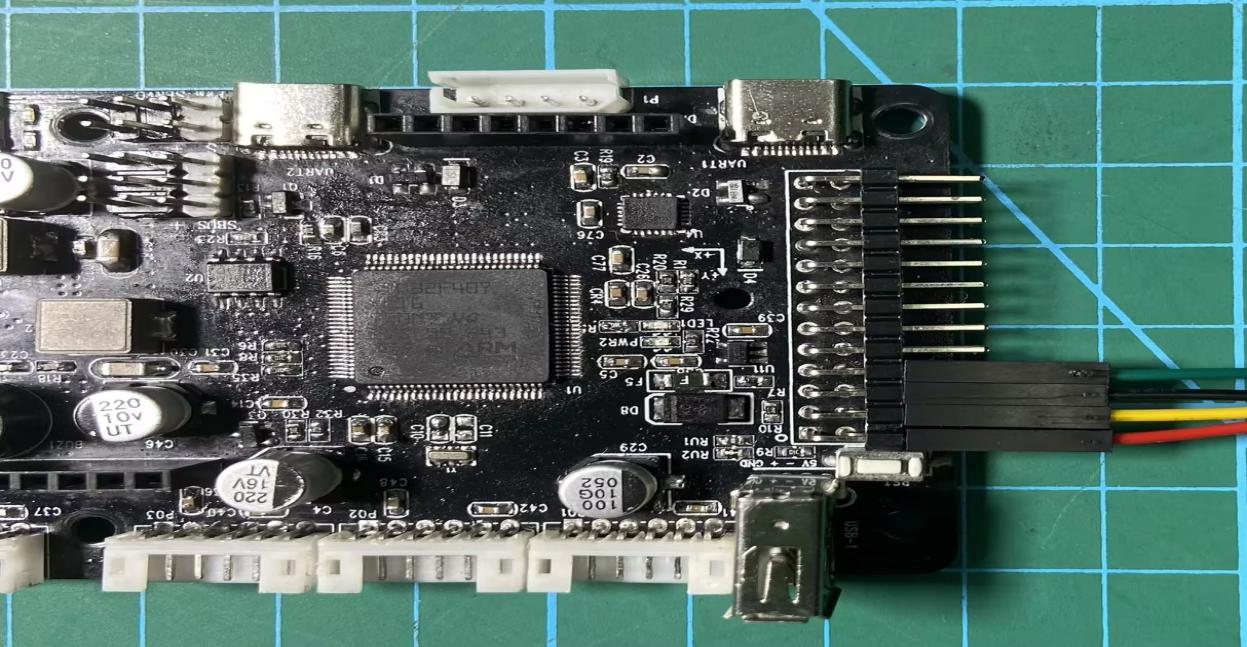
After connecting the Jlink debugger and the Micro-USB data cable, insert the DuPont female connector on the other end of the Jlink into the corresponding pin position on the STM32 main control board:
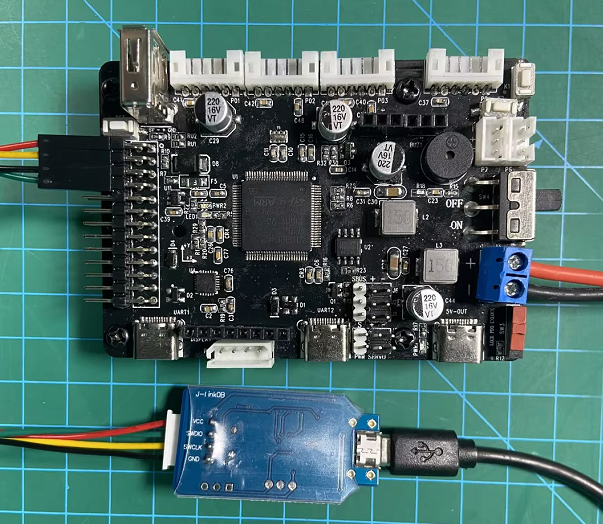
Connect according to the corresponding positions (four wires connected in parallel):
Red VCC connects to the 3V3 pin of the STM32.
Green SWDIO connects to the PA13 pin of the STM32.
Yellow SWCLK connects to the PA14 pin of the STM32.
Black GND connects to the GND pin of the STM32.
The STM32 pin layout is shown in the diagram below:
Download the program: For detailed download methods (Jlink download and Type-C serial port download), refer to ‘2.2.3 Project Compilation & Download’”.
Core Program Analysis
This code is an embedded program based on the STM32 microcontroller, used to control the on/off state of an LED. The program includes several header files, such as main.h, and some library files, such as the GPIO library and the RCC library. In the main function, a series of functions are called to initialize various modules of the STM32 microcontroller, including the system clock, GPIO pins, and the LED.
#include "main.h"int main(void){  // MCU Configuration--------------------------------------------------------  HAL_Init(); //initialize MCU  SystemClock_Config(); // Configure Clock  MX_GPIO_Init(); // initialize GPIO pin  while (1) {
 HAL_GPIO_WritePin(GPIOE, GPIO_PIN_10, GPIO_PIN_RESET); // turn off LED    HAL_Delay(2000);
HAL_GPIO_WritePin(GPIOE, GPIO_PIN_10, GPIO_PIN_SET); // turn on LED    HAL_Delay(2000);  }
}
In the while loop, the LED blinks every 2 seconds by calling the HAL_GPIO_WritePin function and the HAL_Delay function.
In the main function, the program first calls the HAL_Init function to initialize the MCU, and then calls the SystemClock_Config function and the MX_GPIO_Init function to configure the system clock and GPIO pins, respectively. These functions are generated by STM32 CubeMX to initialize various functional modules of the STM32 microcontroller.
In the while loop, the program calls the HAL_GPIO_WritePin function and the HAL_Delay function to make the LED blink every 2 seconds. The HAL_GPIO_WritePin function controls the voltage level of the GPIO pin, turning the LED off and on by passing the GPIO_PIN_RESET and GPIO_PIN_SET parameters, respectively. The HAL_Delay function creates a delay, pausing the program for a specified time before executing the next statement, which in this case, controls the blinking interval of the LED.
Program Outcome
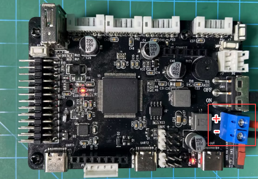
After flashing the program, you can disconnect the Jlink programming cable and provide the STM32 with a 7.4V or 11.4V battery power supply. As shown in the two diagrams below, connect the ‘+’ terminal to the red positive terminal of the lithium battery and the ‘-’ terminal to the negative terminal of the lithium battery.
Effect Diagram 1 (LED Light Off)
Effect Diagram 2 (LED Light On)
2.2.3 Project Compilation & Download
Project Compilation
Once the program is written, we need to compile it into machine language for execution on the embedded system. Keil5 comes with a built-in compiler that can translate program source code into executable files. The compiler can generate different target files based on different processor architectures and instruction sets. Additionally, the compiler can optimize the code to produce more efficient and stable executable files. The process of project compilation involves the following steps:
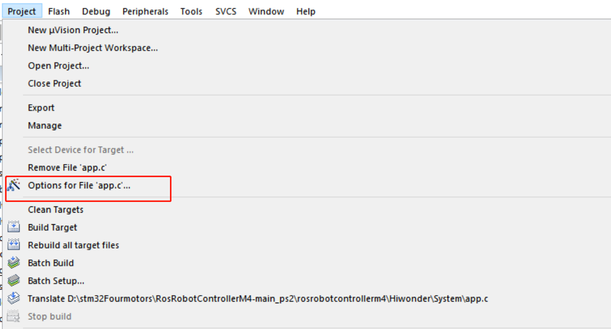
Open the option to generate the hex file in settings:
In the Keil5 software interface menu bar, click on the ‘Project’ option, then click on the ‘Options for File ‘app.c’’ button.
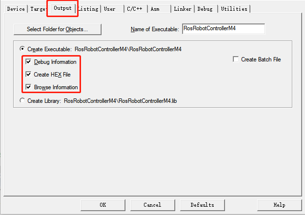
Click on the “OutPut” option, tick the three red options below, and then click “OK”.
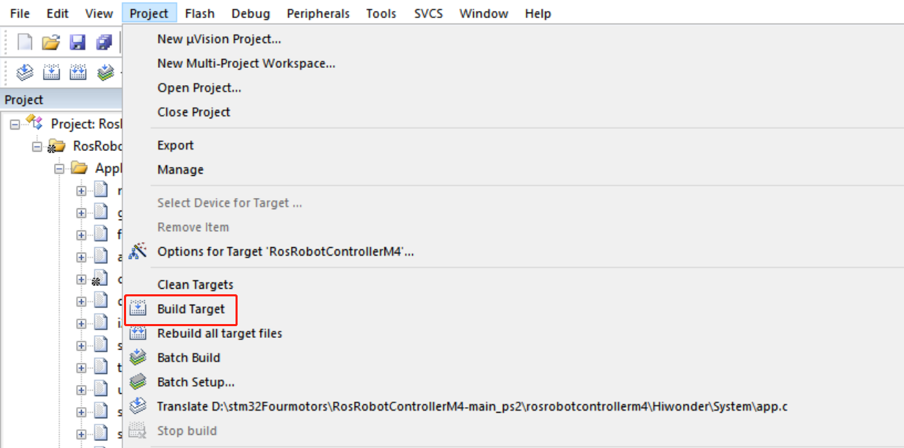
In the Keil5 software interface menu bar, click on the “Project” option, then select “Build Target” from the drop-down menu that appears to compile the project, as shown in the figure below:
You can also compile by clicking on the corresponding icon on the toolbar, as shown in the figure below:

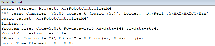
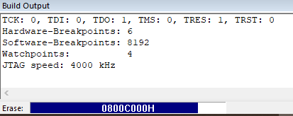
The following message appeared in the “Build Output” window at the bottom of the software, indicating a successful compilation.
Note
Note: If the “Build Output” window displays error message(s) after compiling the project, it is necessary to double-click on the corresponding line to navigate to the relevant position and make corrections. Afterward, compile again. If there are warning message(s), these can be ignored.
USB Download
After compiling the project, you can download the generated hex file to the STM32 main control board. The following software and hardware materials are required.
1. Software & Hardware Preparation
Software: mcuisp (included in the attachments). For specific installation instructions, please refer to “Appendix/Software Installation”.

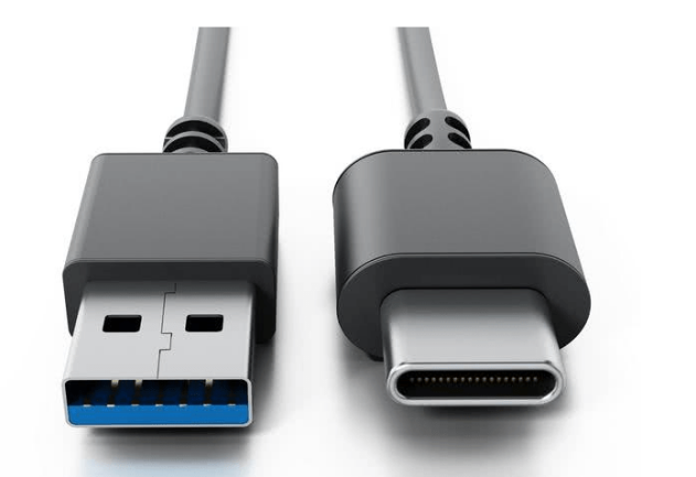
Hardware: Type-C cable and STM32 controller
2. Download Steps
Type-C to USB cable is used to connect the computer and the STM32 main control board (hereinafter referred to as Type-C cable).
STM32 Controller
The specific operation steps are as follows, with the programmed named “Blinking LED”:
(1)Hardware Connection:
Insert the Type-C cable into the Type-C port (UART1) of the STM32 main control board and connect it to the USB port of the computer.
[UART1]
[UART2]
(2)Basic Configuration:
Open the mcuisp software, click on “Search Serial Port” in the menu bar at the top of the software, then set the baud rate (bps) to 115200.
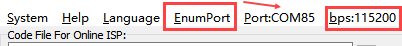
Click on the “STMISP” option in the software interface.
Select “DTR low level reset, RTS high level to enter BootLoader” at the bottom.

(3)Software Burning:
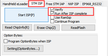
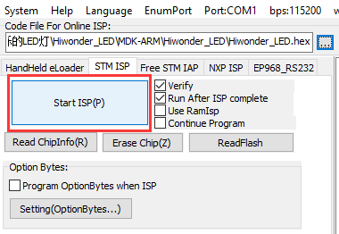
Click on the button inside the red box in the mcuisp software interface, and select the hex file that needs to be burned.


Return to the previous interface and click on the “Start ISP” button to burn the generated hex file onto the STM32 main control board.
Burning in progress
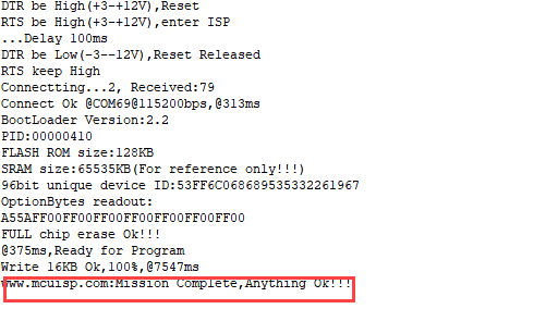
If the sidebar displays the following image, it indicates that the burning process is complete.
Note
Note: The STM32 main control board comes with pre-loaded software (resulting in LED1 blinking blue every 1 second). If you need to burn the PS2 joystick control program, you can find the RosRobotControllerM4.hex file in the ‘Chapter 1: Introduction to the Car Hardware and Usage / Section 2: PS2 Joystick Remote Control / Program / rosrobotcontrollerm4_motor_ps2 / MDK-ARM / RosRobotControllerM4’ folder for burning.
If burning fails, refer to the ‘Troubleshooting Guide’ document in the ‘Appendix’ folder for assistance.
Note
Note: To avoid any abnormal occurrences during the burning process, users should follow the steps in sequence carefully!!!
2.2.4 SWD Simulation Debugging
Preface
After the program is written, it can be tested through simulation debugging. There are two debugging methods available on the STM32:
JTAG (Traditional Debugging Method): Primarily used for internal chip testing. Most advanced devices, such as DSPs and FPGAs, support the JTAG protocol.
SWD Debugging (Serial Debugging): A communication protocol for ARM core debuggers. Compared to the JTAG protocol, SWD debugging uses fewer port resources. This article will introduce the SWD debugging method.
Debugging Instructions
Software Preparation: Keil5 software (refer to previous sections for installation and compilation methods).
Jlink driver (found and installed from the “Attachments/Software Installation/Jlink Driver” folder).
Hardware preparation: Jlink emulator (self-supplied, with Dupont wires) and a MicroUSB cable.
1. Hardware Connection:
Connect Jlink to the stm32 controller as below:
The wiring guidelines are as follows:
VCC (red) -> 3V3
SWCLK (yellow) -> PA14
GND (black) -> GND
SWDIO (green) -> PA13
After completing the wiring, you can start software debugging.
2. Set Up Debugging Environment
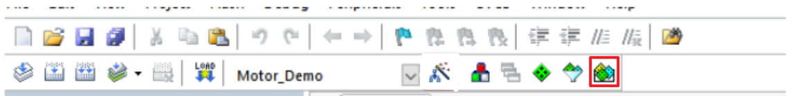
Open the Keil5 software and click the button on the icon to enter the environment configuration interface.

Click the “Debug” button, then select “J-LINK/J-TRACE Cortex” from the “Use” dropdown menu.
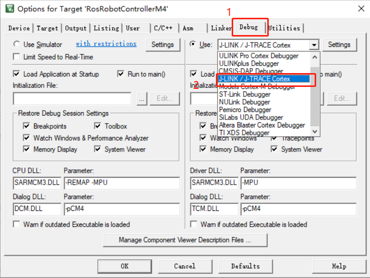
Click-on ‘Settings’ to initiate configuration.
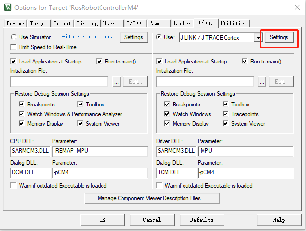
In the “SN” option, the serial number will be automatically recognized. Select it or keep the default setting. Then, in the “Port” option below, select “SW” and finally click “OK”.
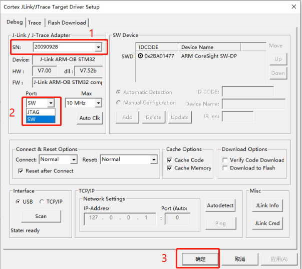
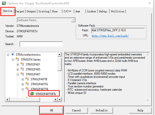
Return to the previous interface, click “Device”, select the corresponding chip model, and then click “OK”.
3. Debug
Click the “Debug” button on the Keil5 software interface to enter the debugging interface.

If the “Output” pane at the bottom displays the debugging loading process and no errors occur, it indicates normal operation.
>> Debugging Program Execution
In the debug interface toolbar (as shown below), the contents within the red box, from left to right:
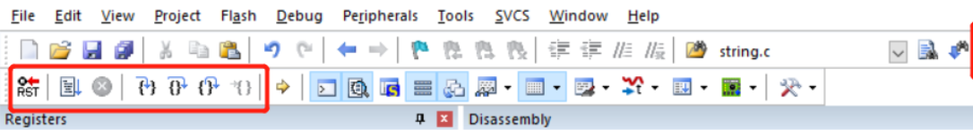
Reset: Resets the program; the reset type triggered depends on the configuration of the burner.
Run: Starts the current program to run at full speed until it encounters a breakpoint.
Stop: When the program is running at full speed, clicking this button stops the program. It stops where the program is currently executing.
Step (F11): Executes a single statement according to the current debugging window’s language. If encountering a function, it steps into the function. If in the disassembly window, it executes only one assembly instruction.
Step Over (F10): If in a C language window, it executes one statement at a time. Unlike step debugging, it does not step into functions but runs them at full speed and jumps to the next statement.
Step Out: If in a C language window, it runs all the contents after the current function at full speed until returning to the previous level.
Run to Cursor Line.
Variable Checking

The button in the image above is the variable monitoring button, used to observe the assignment of variables during program execution.
Example:
Pay attention to the msg variable in the program (users can choose the values they want to observe as examples during debugging).

After selecting the msg variable, right-click and choose “Add ‘msg’ to”, then select the observation window Watch1 or Watch2.
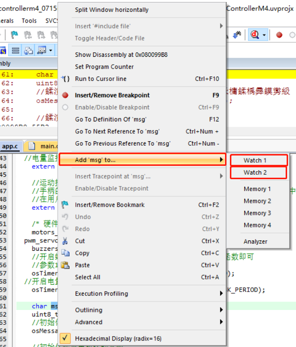
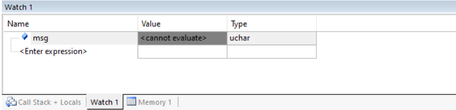
You can now observe the real-time value of msg in the Watch1 window below.
Note
Note: To address any potential anomalies during the debugging process, users should follow the steps in order!
2.2.5 Using a LED Blinking Program with FreeRTOS
Program Logic
This experiment utilizes the FreeRTOS operating system to create a user task. Within this task, the PE10 pin’s high and low levels are manipulated to control the blinking of an LED.
Hardware Connection
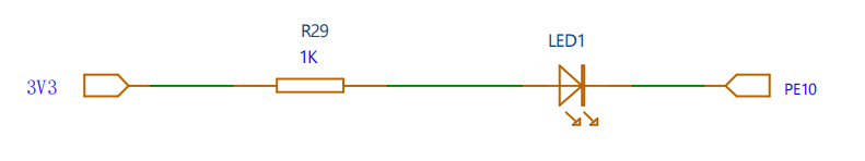
The LED is connected to pin PE10, where it is off when the pin is at a high level and on when it is at a low level.
Below is the circuit diagram:
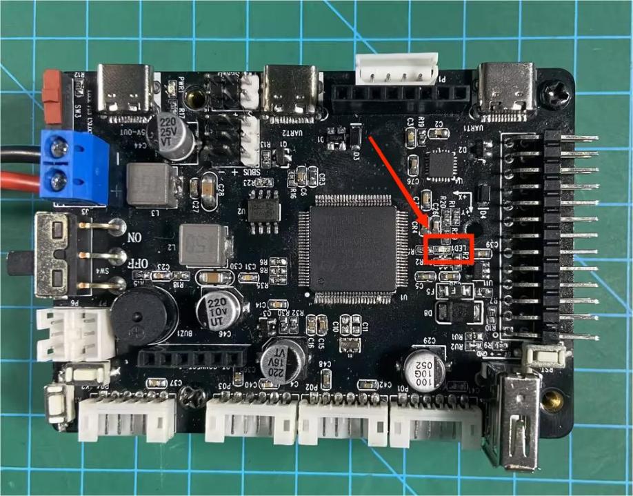
The LED on the controller is as below:
Program Download
The example program for this section is named “Hiwonder_FreeRTOS_LED”.
Project Creation and Program Writing
1. Project Creation
After double-clicking to open the STM32CubeMX software, the following interface will appear:
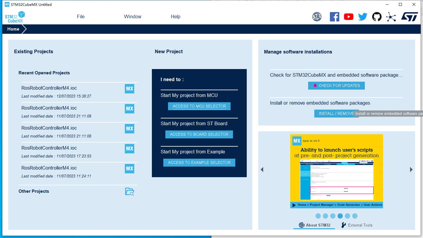
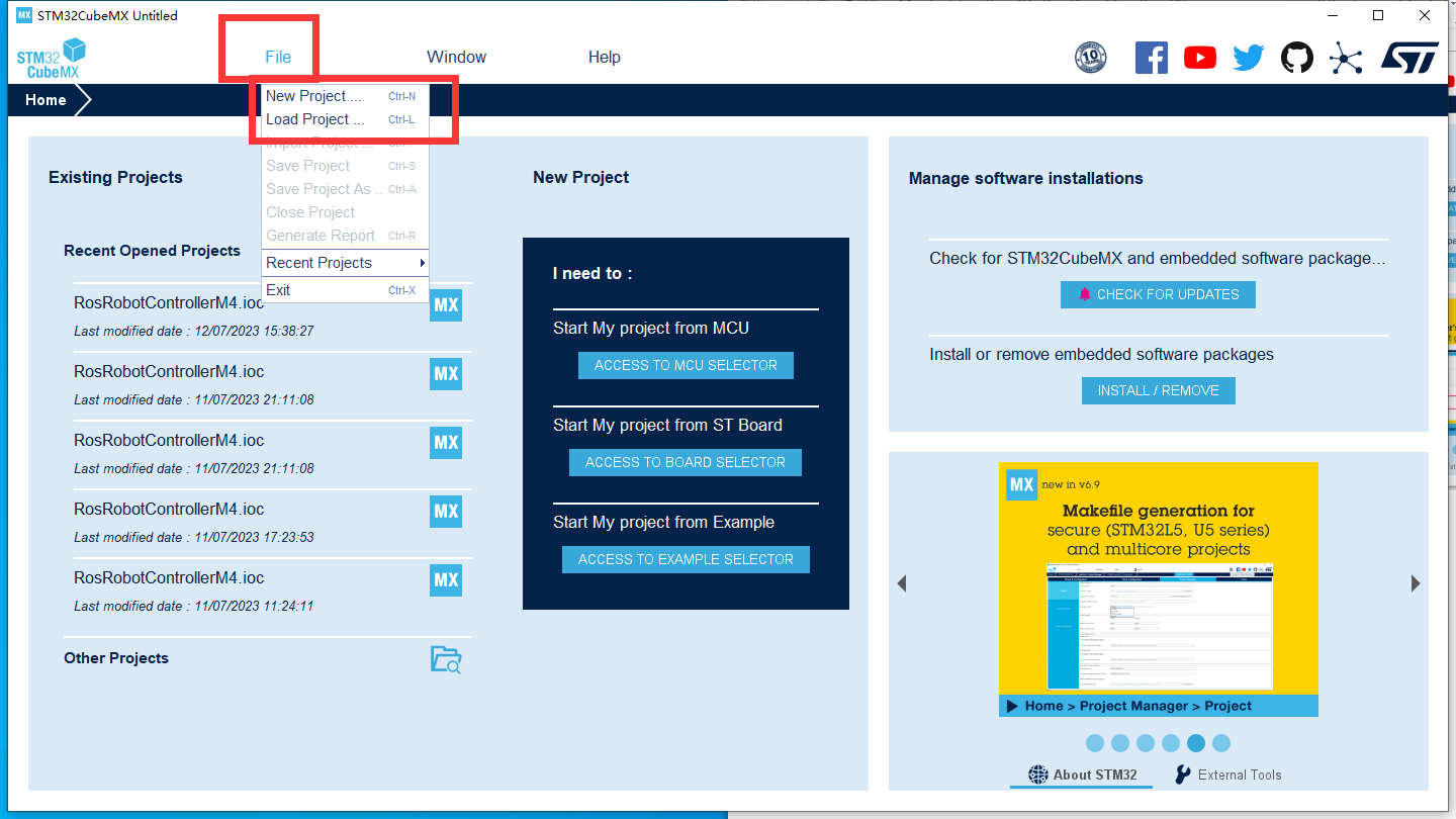
Click on “File”. If you already have a project created by STM32CubeMX, you can click on the second option “Load Project…”; if you want to create a new project, click on the first option “New Project”.
Wait for the plugins to finish loading.
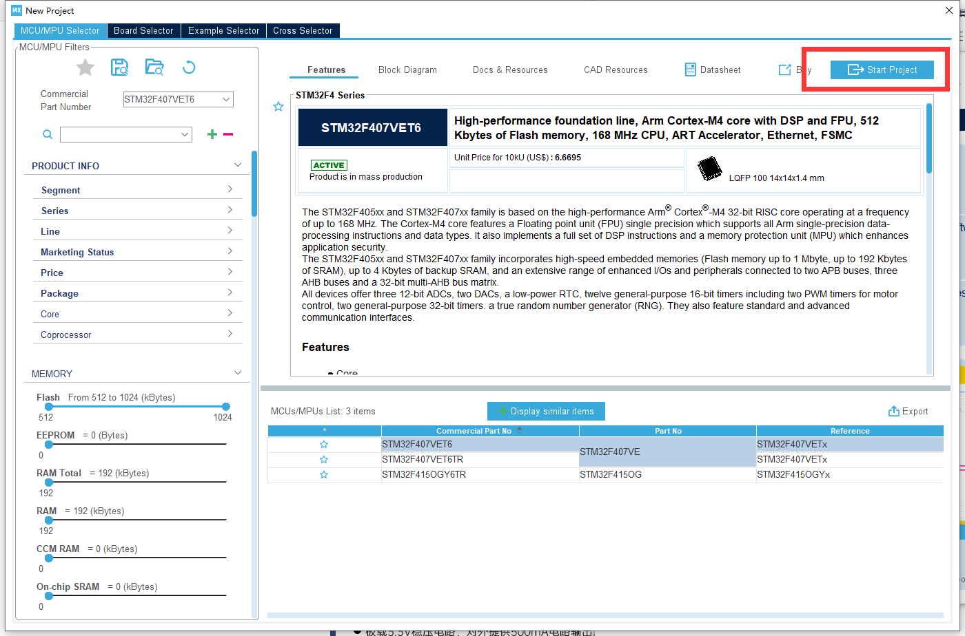
In the input box below, enter the selected chip model: STM32F407VET6
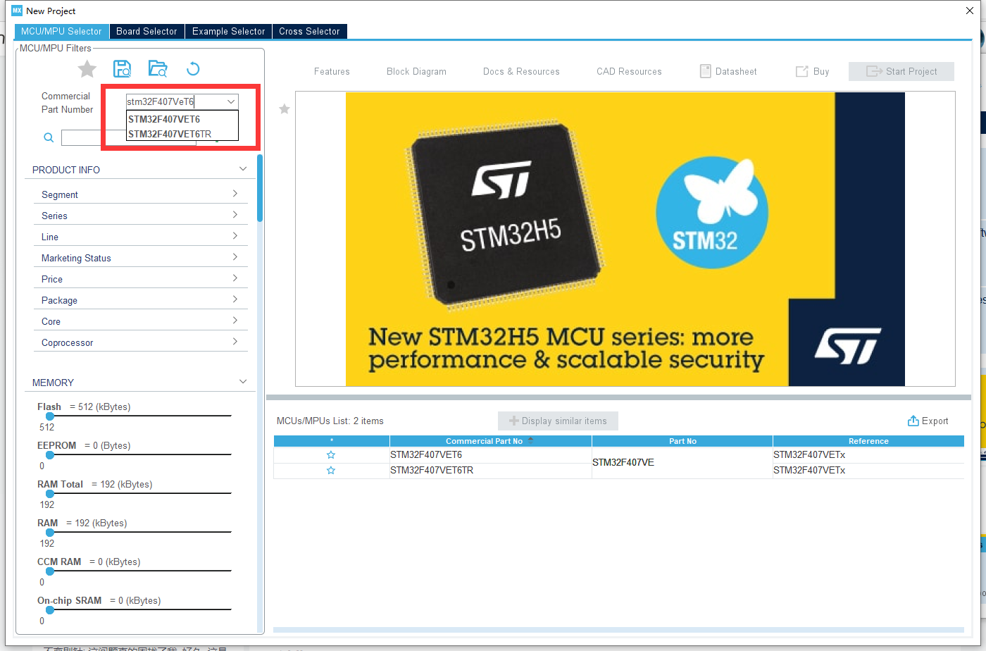
After selecting the chip, you can choose the necessary chip information in this box.
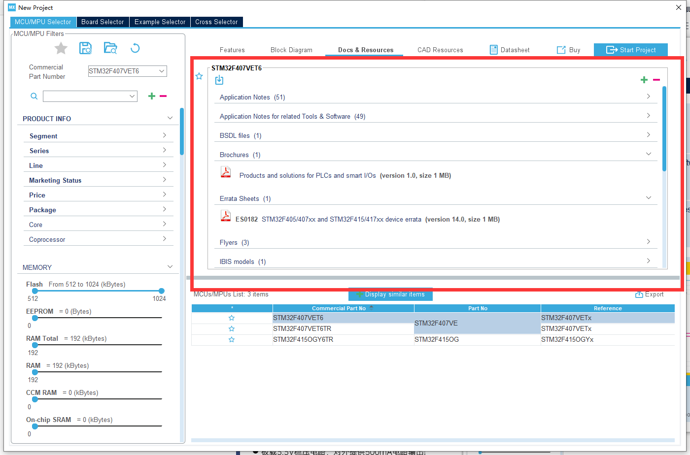
Then click on “Start Project” to begin creating a new project.
2. Chip Configuration & Project Creating
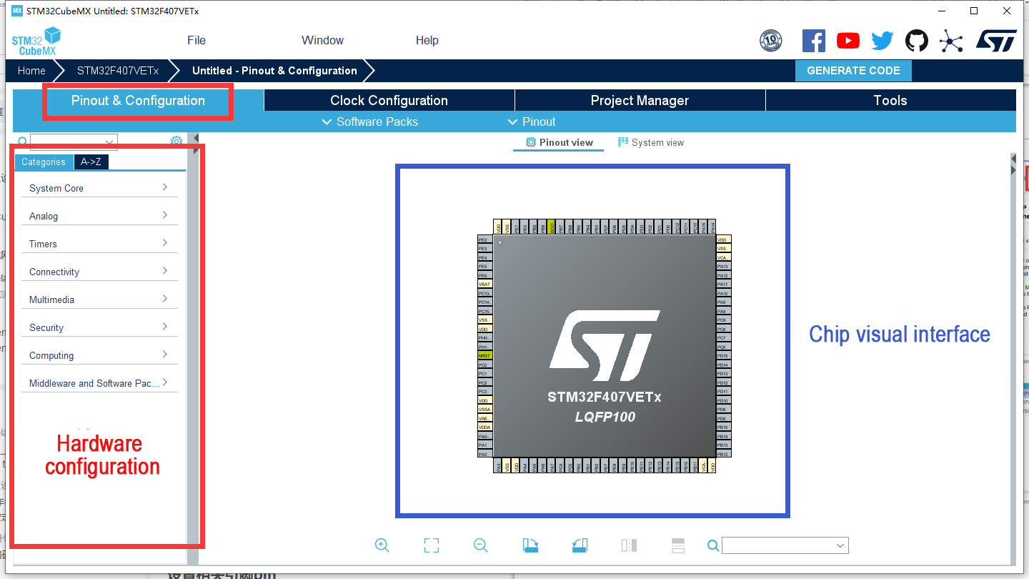
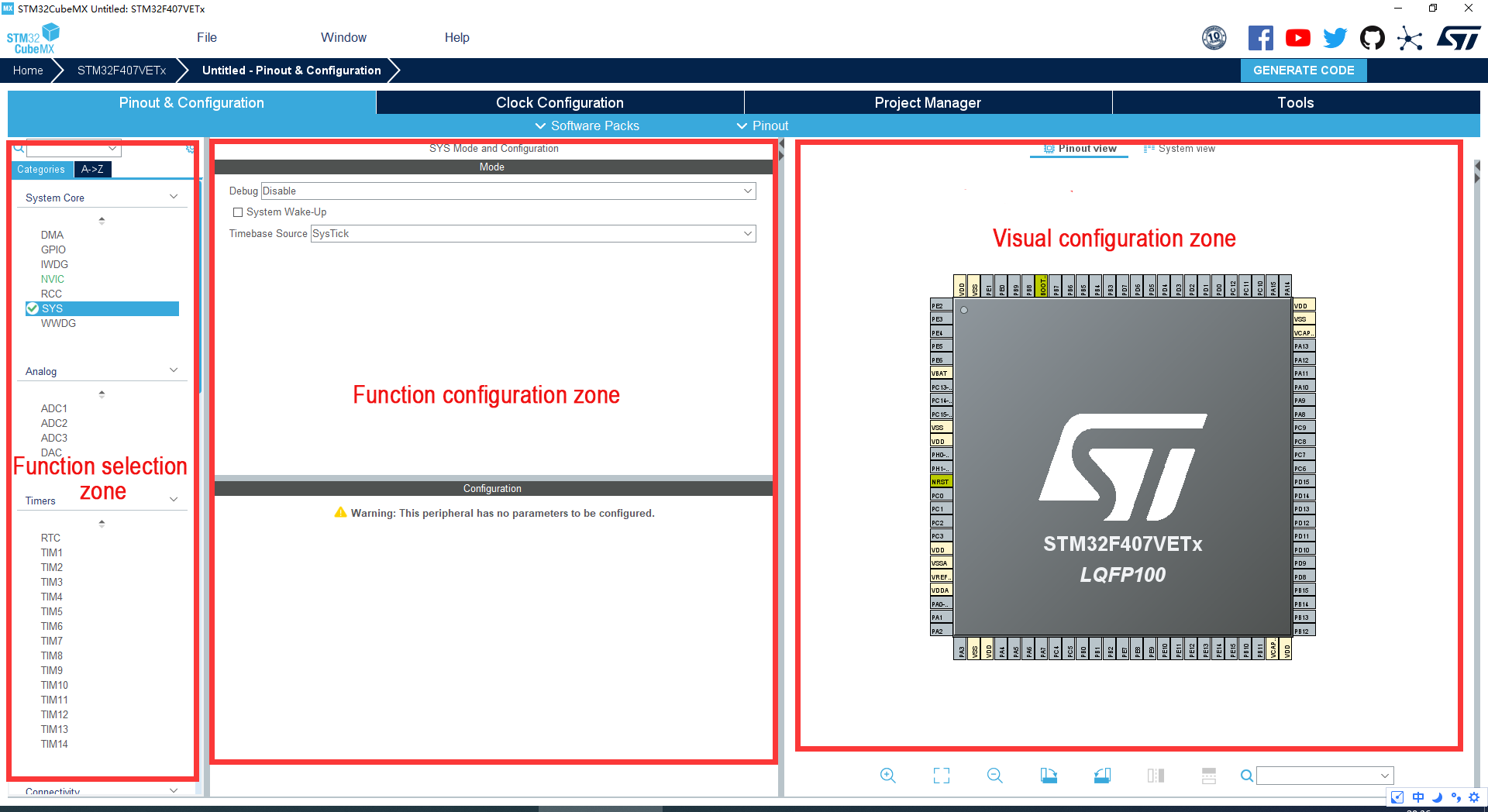
(1) Chip Configuration Interface
① Pinout & Configuration :
On the left are hardware configuration options, and on the right is the visual interface for chip operation, where you can configure the IO ports.
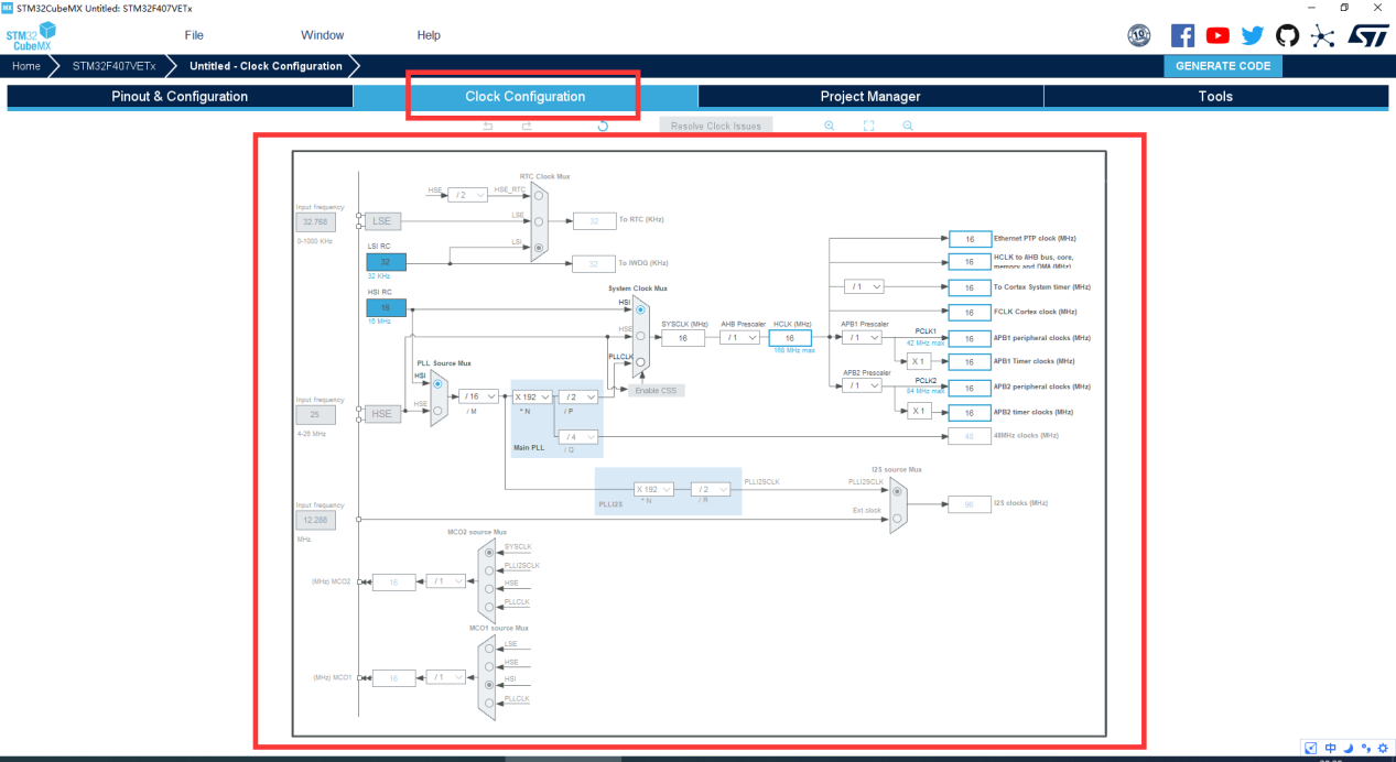
Clock Configuration:
This interface is for configuring the clock of various parts of the chip.
Project Manager:
This interface is the project management interface, where various parameters for generating project files are configured.
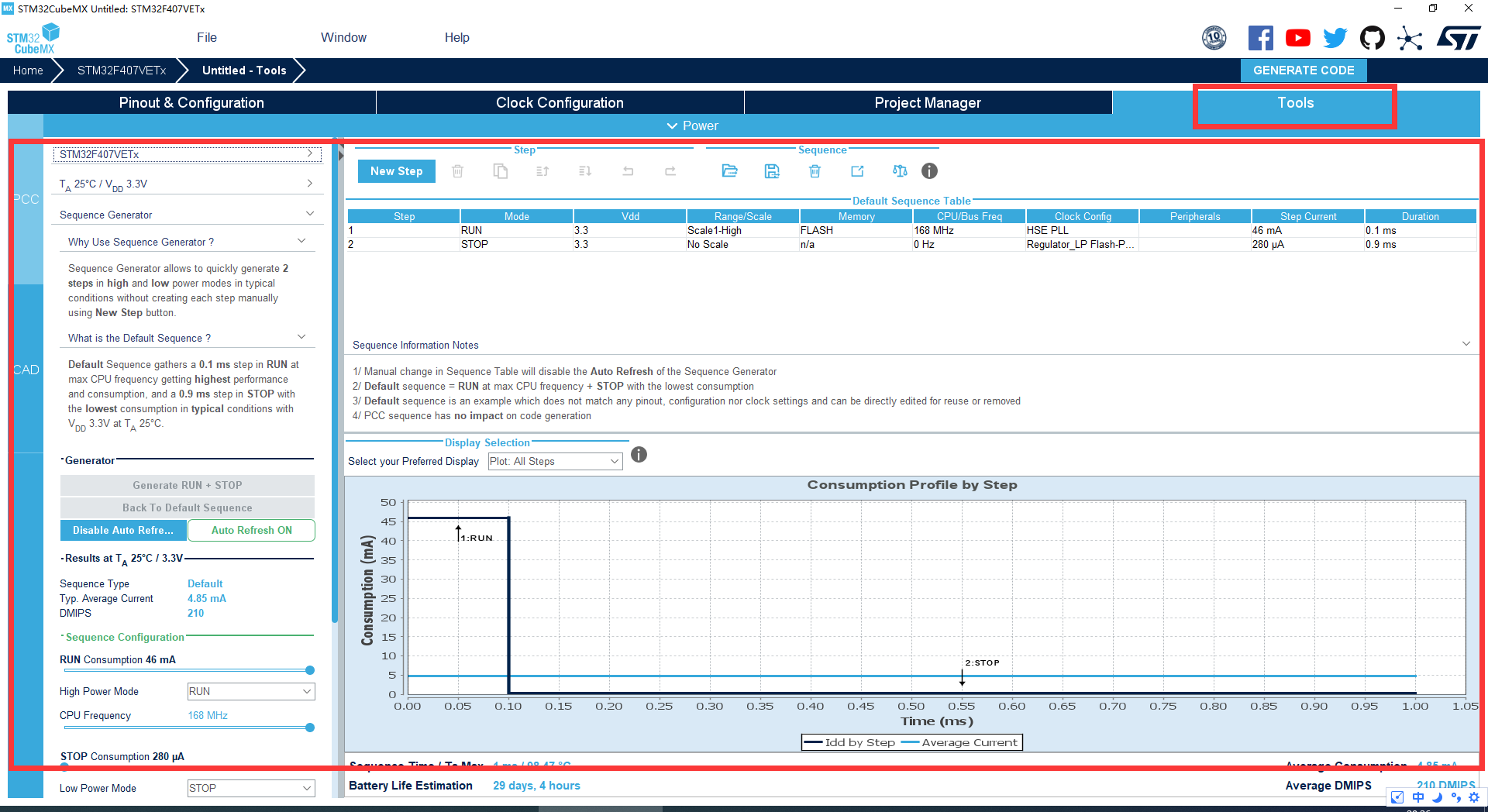
Tools:
This interface is the tools interface, where these tools can be used during the development process.
(2) Pinout & Configuration Interface Configuration
Click on “Middle and Software Packs”, choose “FreeRTOS”, then select the CMSIS_V2 version to use FreeRTOS in the project.
Configure the relevant parameters of the RTOS system in the configuration.
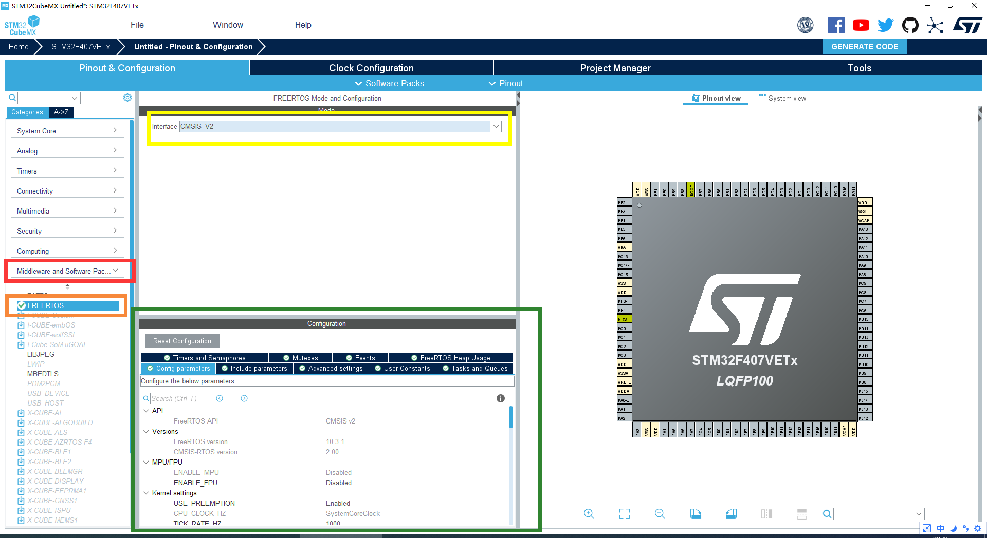
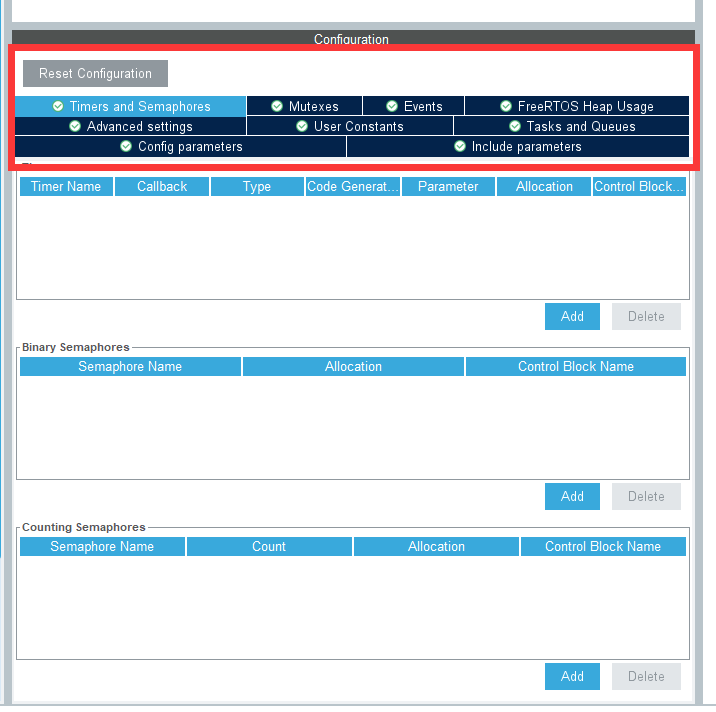
In the Configuration box, there are many options for creating system functionalities:
Timers and Semaphores: Create timers and semaphores.
Mutexes: Create mutexes.
Events: Create events.
FreeRTOS Heap Usage: Set up the heap for the system and tasks.
Advanced Settings: Advanced system settings.
User Constants: Create user constants.
Tasks and Queues: Create tasks and queues.
Config Parameters: Configure the system kernel.
Include Parameters: Configure the system include program.
Create Task
Select the “Tasks and Queues” option, then click “Add” in the Task section to add a task.
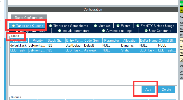
The task creation interface is as below:
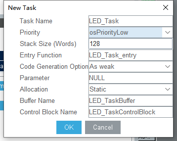
Task Name: The name of the task, where you can define your own task name.
Priority: The priority of the task, usually set to default.
Stack Size: The size of the task’s stack, typically set to default.
Entry Function: The entry function of the task, where you write the task loop. You can name it as you wish.
Code Generation Option: Generates virtual function code for the task’s entry function.
Parameter: Input parameters, usually set to NULL.
Allocation: The allocation method for the task, either dynamic or static. Here, we choose to create a static task.
Buffer Name: The name of the task’s buffer, usually set to default.
Control Block Name: The name of the task’s control block, usually set to default.
After configuring, click “OK” to create the task.
Configure IO Port
One end of the LED on the development board is connected to 3.3V, and the other end is connected to the PE10 pin. Therefore, we need to configure the PE10 pin. When the pin is high, the LED is off (not conducting); when the pin is low, the LED is on (conducting).
Click on the PE10 pin in the visual interface and set it to GPIO_Output.
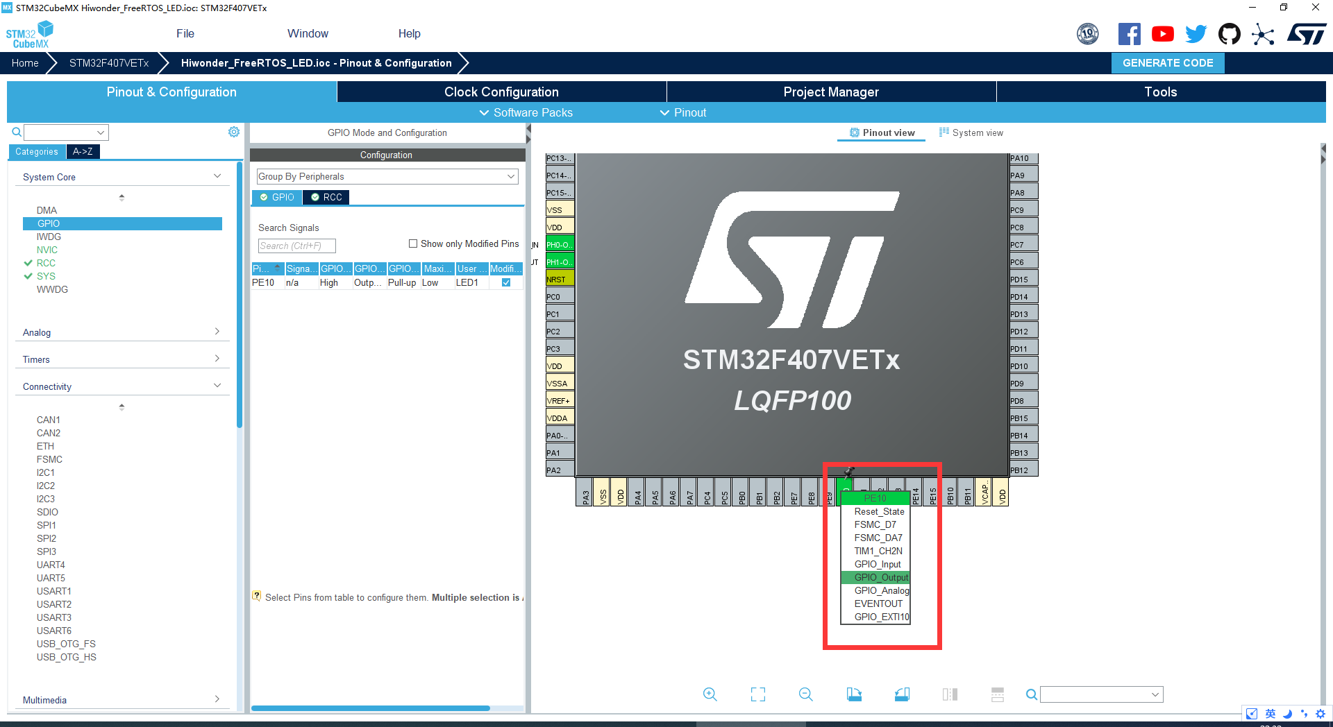
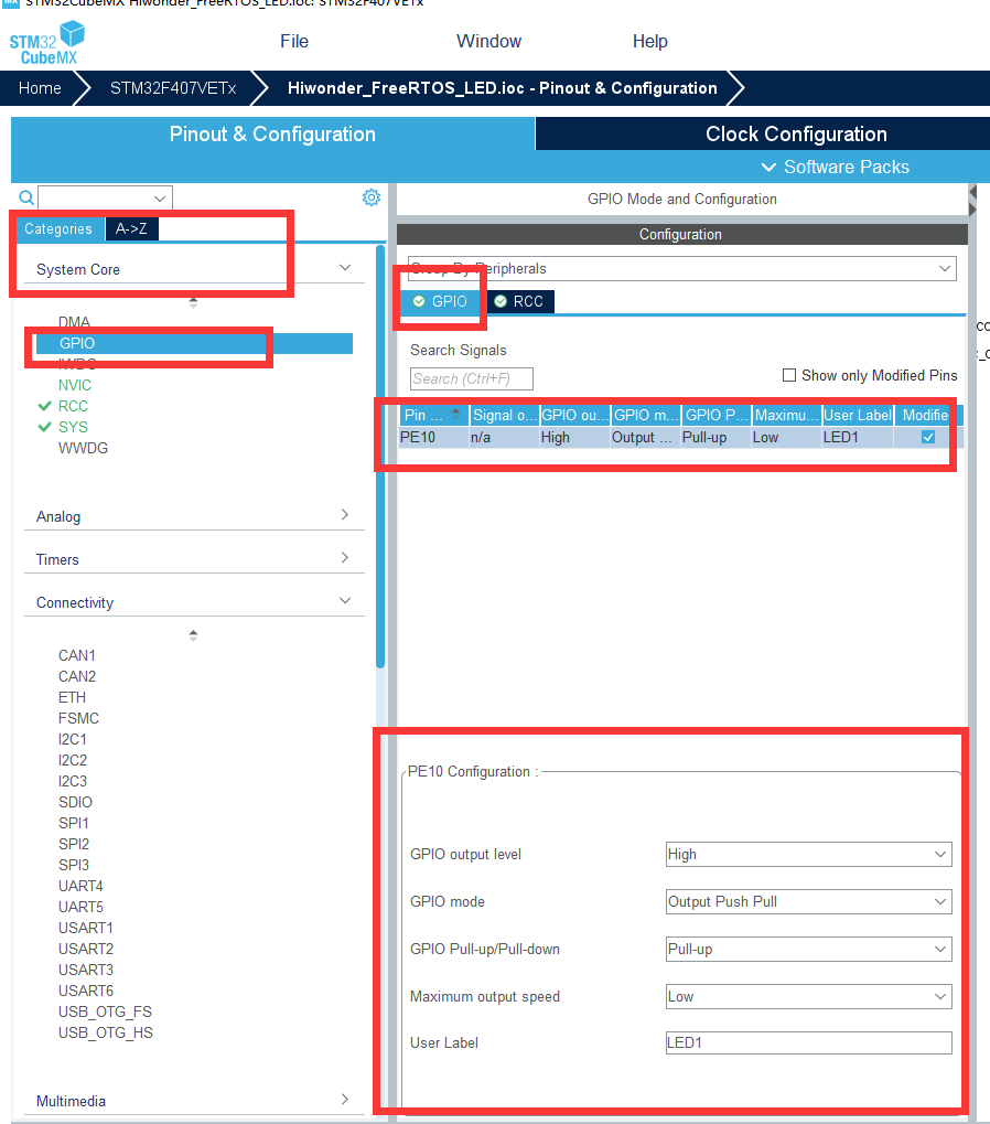
Select the “System Core” dropdown menu, click on the “GPIO” option, and configure it as follows:
Default output: High
Output mode: Output Push Pull
Pull: Pull-up
Output speed: Low
User-defined label: LED1 (you can name this as you wish, and it will be associated with the IO macro definition in the program).
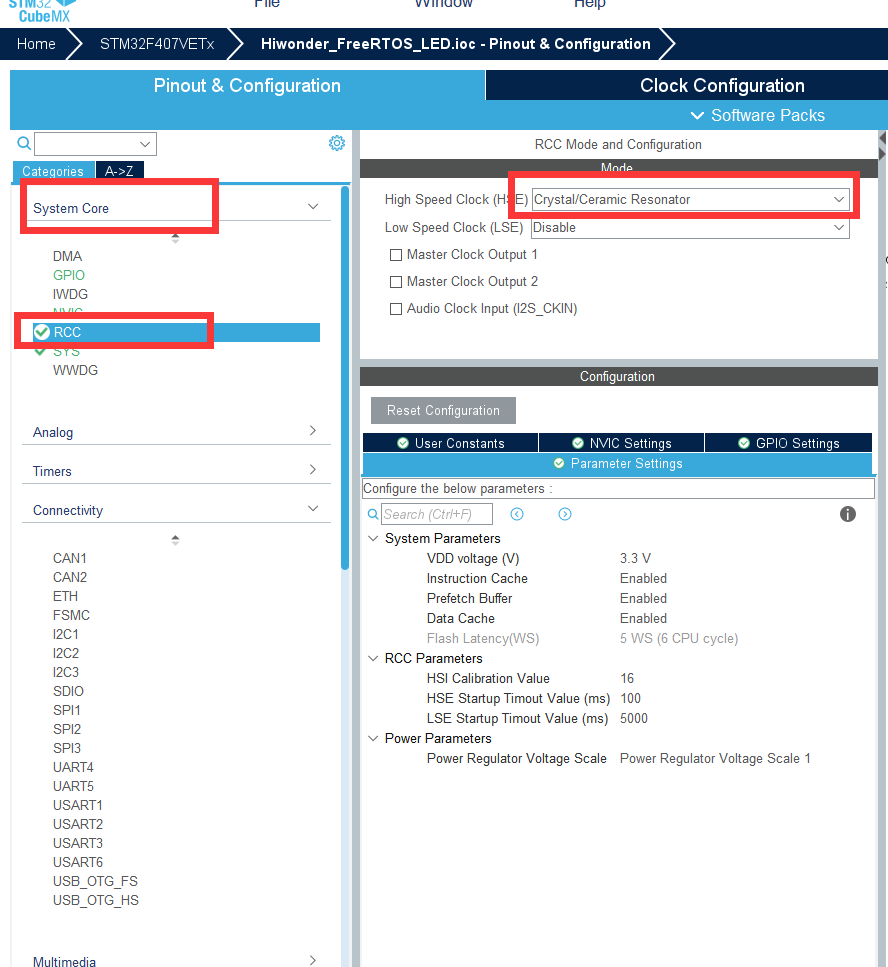
Configure RCC
Click on the RCC option, select External High Speed Clock (HSE) as Crystal/Ceramic Resonator (passive external oscillator).
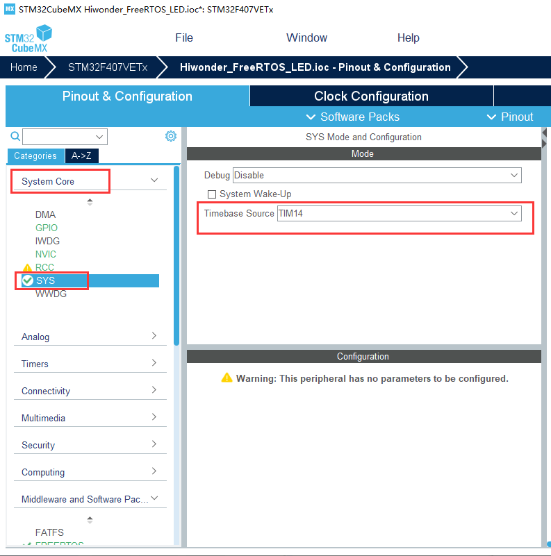
Configure SYS
Select TIM14 (Timer 14) as the system clock.
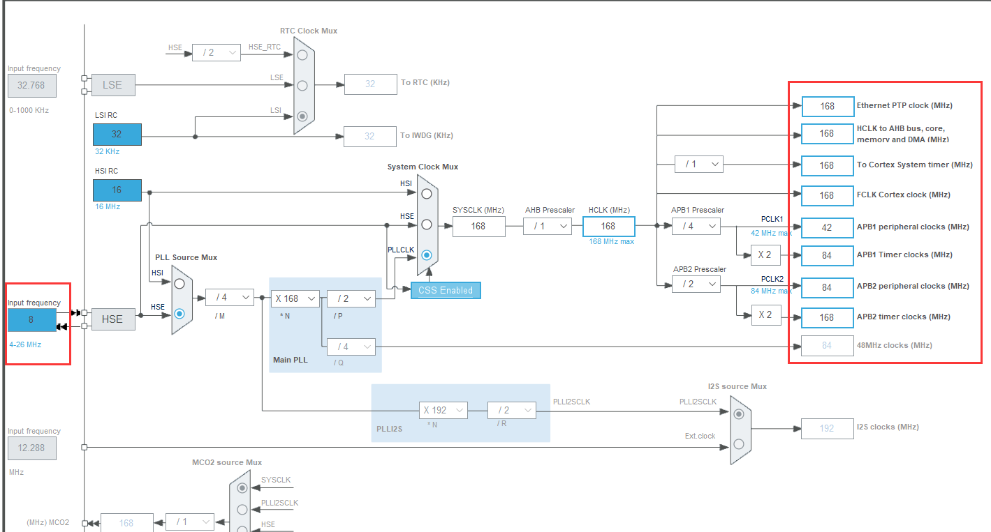
Clock Configuration Interface Configuration
Click on “Clock Configuration”. The external oscillator of the development board is 8 MHz, so enter 8 in the “Input frequency” field, then configure according to the diagram below.
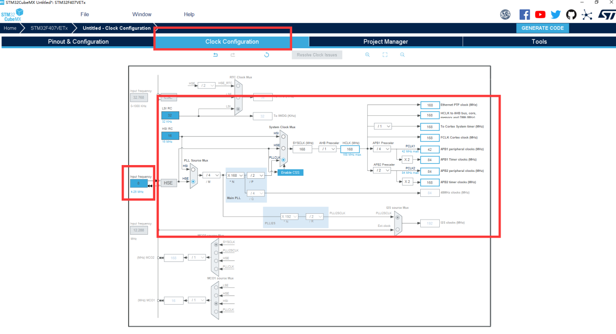
You only need to focus on the parameters at the end that will be used in the projects.
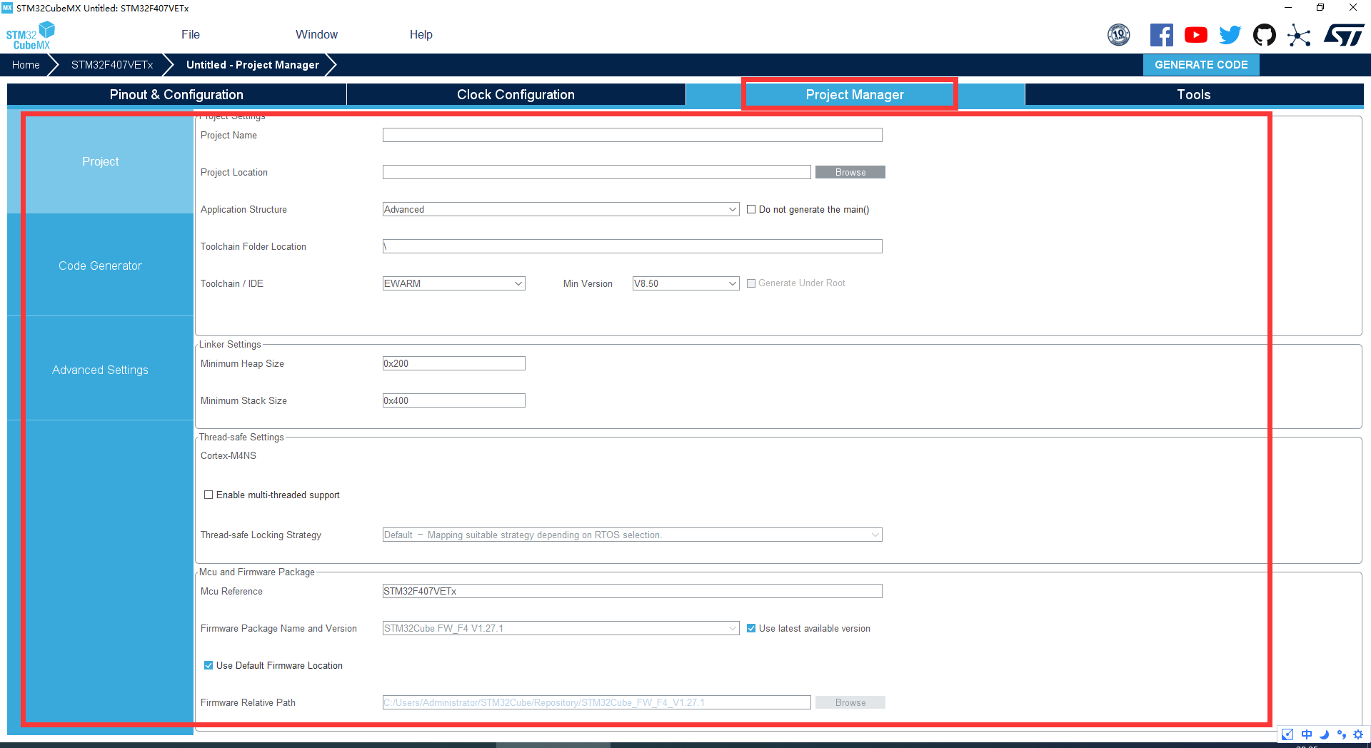
Project Manage Interface Configuration
Click on “Project Manager” to enter the project generation configuration, focusing mainly on the “Project Settings” under the “Project” tab.
Project Name: Name of the project
Project Location: Local path for the project
Application Structure: Choose “Basic”
Toolchain Folder Location: Default location
Toolchain / IDE: Choose the programming and compiling tool. We are using Keil5 for programming, so select “MDK-ARM”
Min Version: Select the minimum version as “V5”
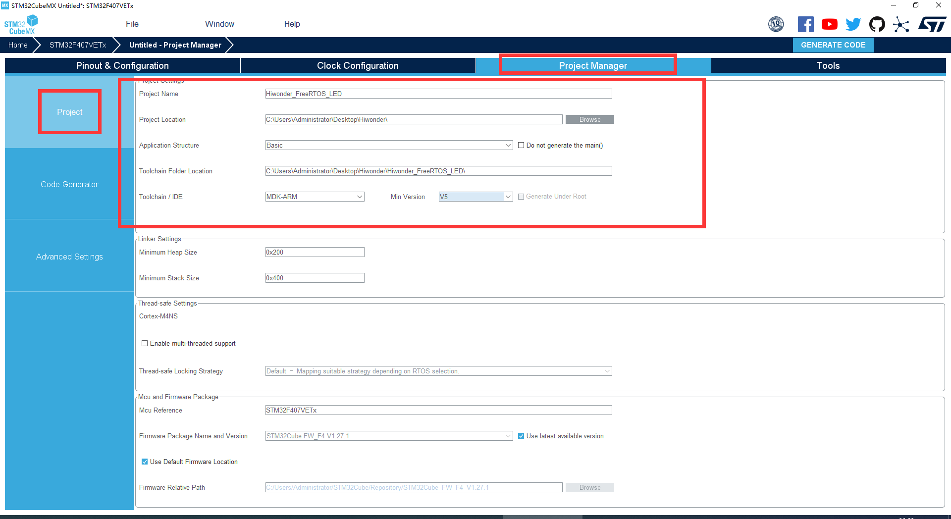
Click-on ‘GENERATE CODE’ button at the upper right corner.
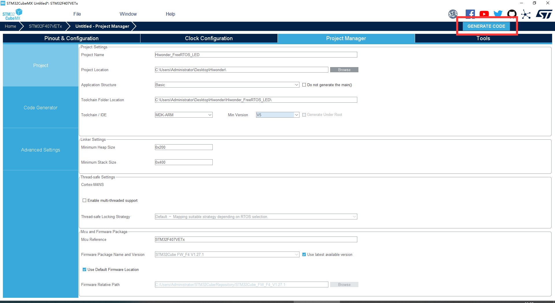
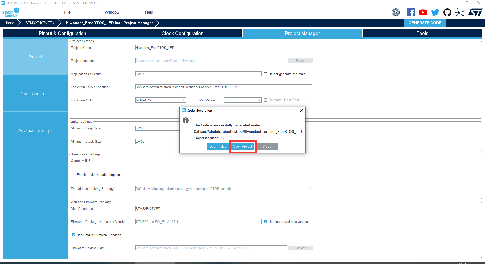
After generation, click “Open Project” to directly open the project with Keil5 software (Keil5 needs to be installed).
3. LED Program Editing
Open main.c file in Application / User.
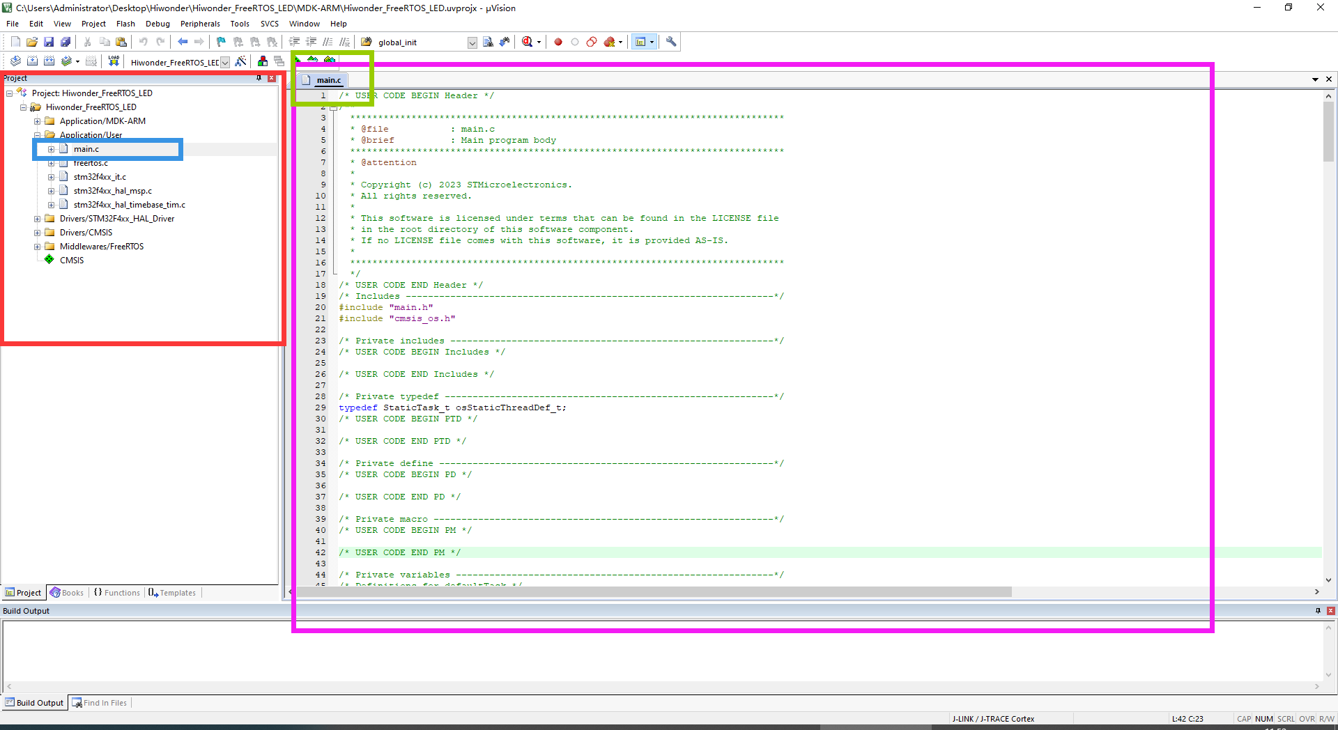
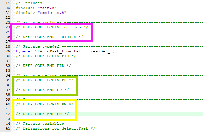
For project files generated by STM32CubeMX, users’ program code and comments need to be added or modified within specific ranges, as shown below:
/* USER CODE BEGIN xxx*/
//User comments and program code
/* USER CODE END xxx*/
If modifications are made outside of this range, they will be overwritten during the next configuration modification and regeneration in STM32CubeMX. Only the code and comments within this range will be preserved.
For files created and added manually, this restriction does not apply.
Note
Note: If you manually add this tag, STM32CubeMX software will not recognize it and will still overwrite the code outside of this range.
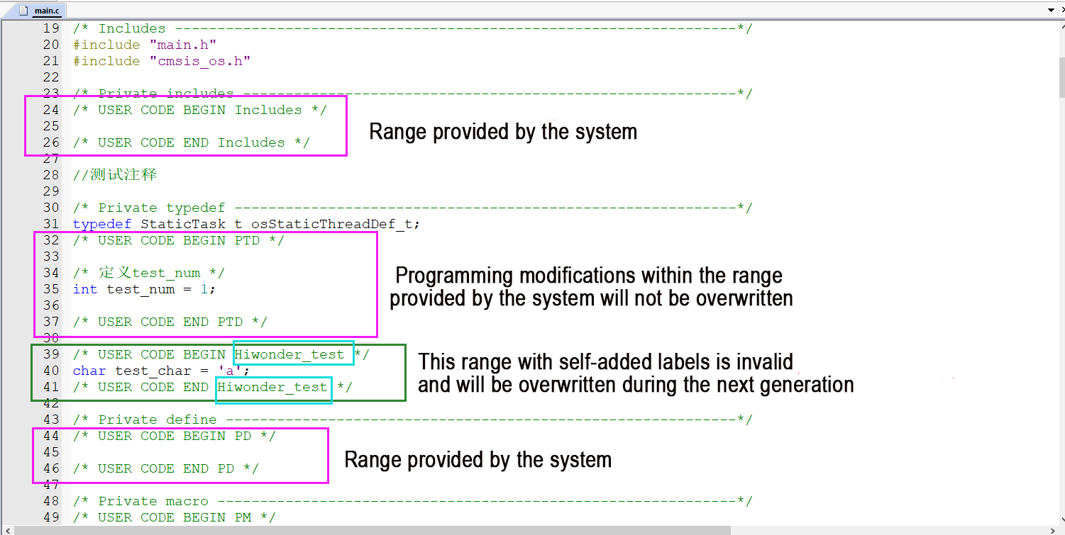
The while loop in the main() function will not be reached by the system, so LED programs cannot be written here.
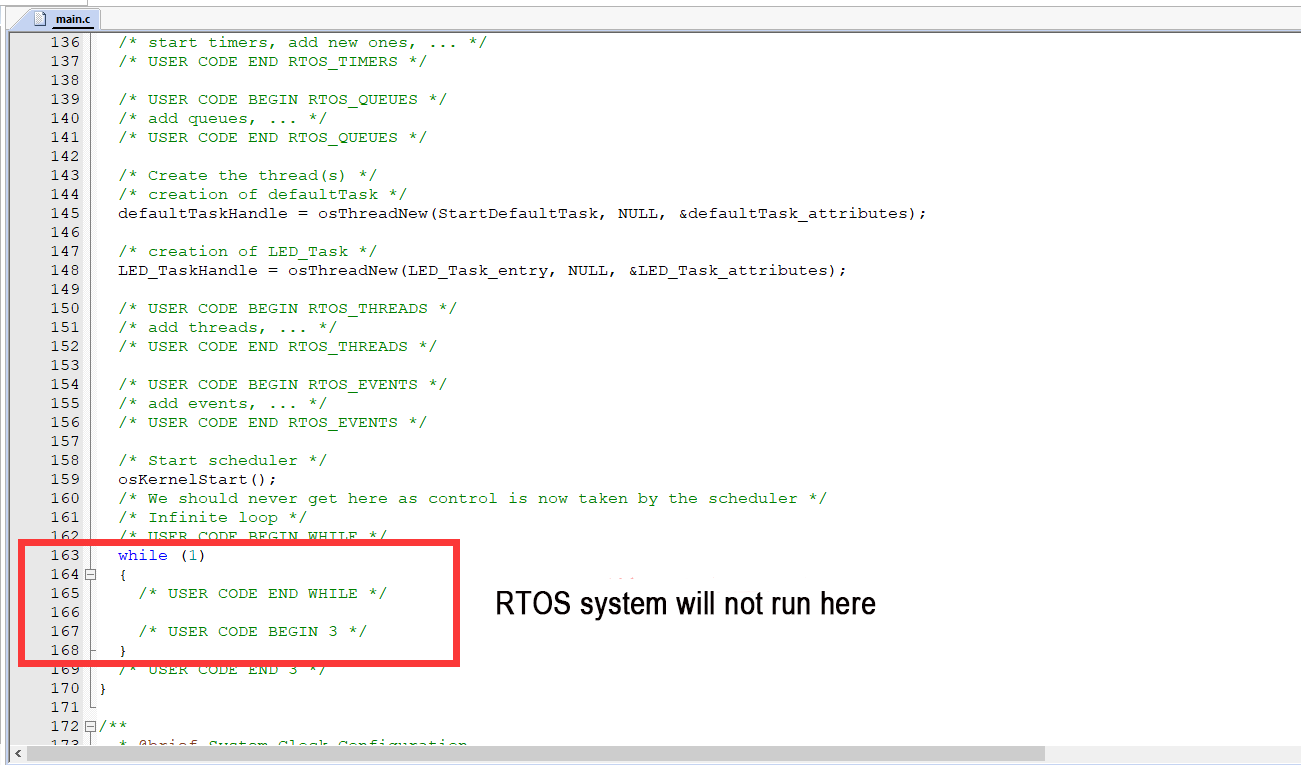
You need to find the LED_Task_entry() function that we defined as the task entry function when configuring the FreeRTOS system (section 2.3). Write your LED blinking logic inside this task function.
In the main.c file, you can find the declaration and virtual function definition of the LED_Task_entry() function.
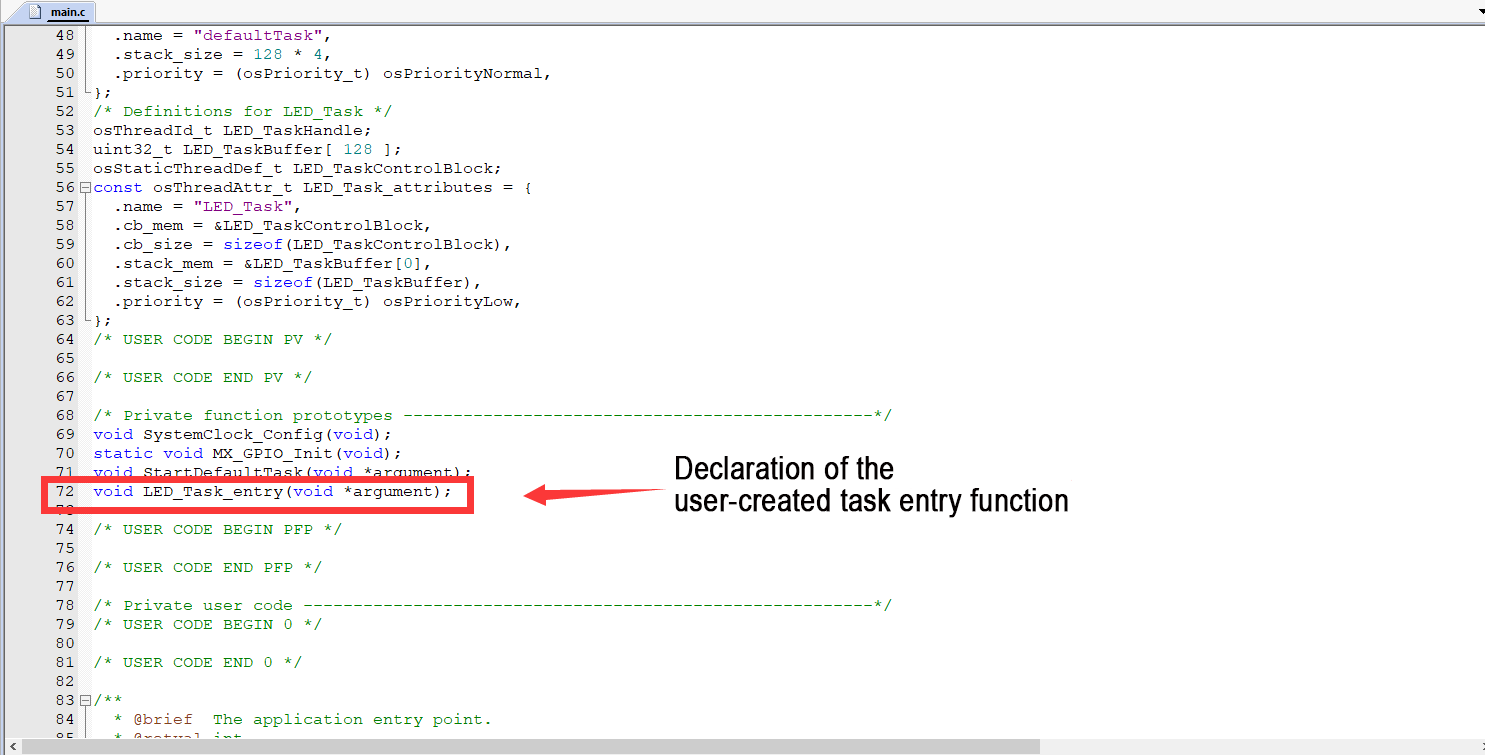
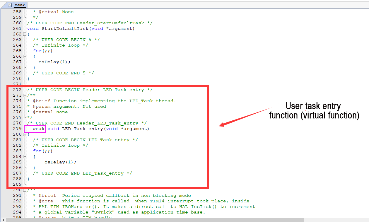
Our LED blinking program can be placed inside this function. Make sure to write it within the range provided by the system for ease of reconfiguration later.
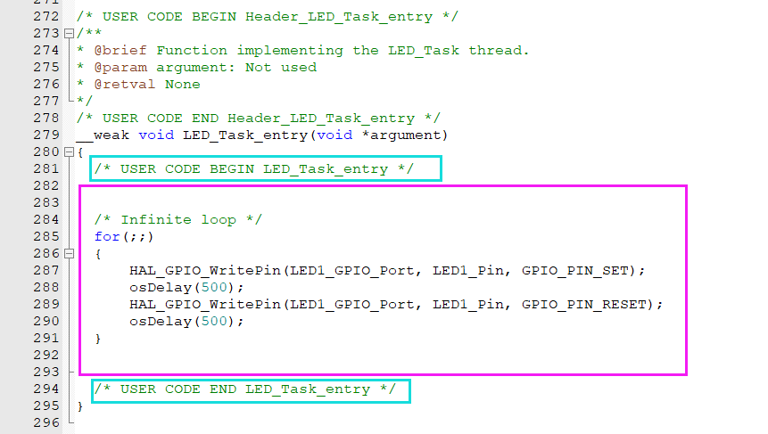
Program logic:
for( ; ; ){
Set the LED pin to high level;
    Delay for 500ms;
    Set the LED pin to low level;
    Delay for 500ms;
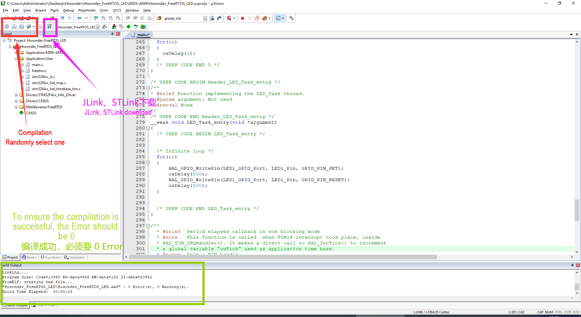
After compilation, once there are no errors indicated below, you can proceed to download and burn the program.
2.3 RosRobot Controller Program Analysis
Please click ROS Robot Control Board->3.RosRobot Controller Program Analysis to get the Docker Container Course.